
Sputtering target of oxide semiconductors and the manufacturing methods of oxide semiconductor layers

a technology of oxide semiconductors and manufacturing methods, which is applied in the direction of oxide conductors, non-metal conductors, conductors, etc., can solve the problems of donor adversely mixing into the sintered body as an impurity, and the problem of 0.1 to 1.0 wt % aluminium (al) of about 0.1 to 1.0 wt %, etc., to achieve stable quality, low cost, and high quality

Active Publication Date: 2015-04-14
HITACHI METALS LTD
View PDF13 Cites 2 Cited by
  • Summary
  • Abstract
  • Description
  • Claims
  • Application Information

AI Technical Summary

Benefits of technology

[0014]A preferred aim of the present invention is to provide a technique capable of forming an oxide semiconductor target with a high quality in a low cost.
[0015]Also, another preferred aim of the present invention is to provide a technique capable of obtaining a stable quality in an oxide semiconductor film formed with using an oxide semiconductor target.
[0021]An oxide semiconductor target with a high quality in a low cost can be formed. Also, in an oxide semiconductor film formed with using the oxide semiconductor target, a stable quality can be obtained.

Problems solved by technology

However, from studies made by the inventors of the present application, problems described below have been found out.
However, a material of the crushing ball introduced into the ball mill is alumina (Al2O3), and therefore, aluminium (Al) of about 0.1 to 1.0 wt % (0.3 to 3.2 at %) to be a donor is adversely mixed into the sintered body as an impurity.
If the sintered body is used as the target in the sputtering method, the Al is adversely added to the formed oxide semiconductor film as the impurity.
Therefore, in the thin-film transistor in which the oxide semiconductor film is adopted for the channel layer, the oxide semiconductor film cannot be functioned as a semiconductor, and therefore, a problem such that the off operation is impossible in the thin-film transistor arises.
However, any consideration results in increase of the manufacturing cost.

Method used


Image

  • Sputtering target of oxide semiconductors and the manufacturing methods of oxide semiconductor layers
  • Sputtering target of oxide semiconductors and the manufacturing methods of oxide semiconductor layers
  • Sputtering target of oxide semiconductors and the manufacturing methods of oxide semiconductor layers

Examples


first embodiment

[0041](First Embodiment)

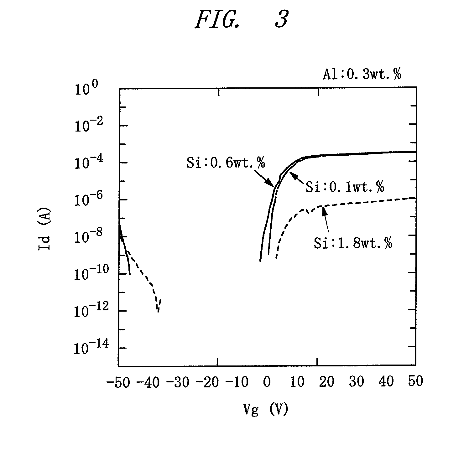
[0042]In the invention of the present application, by adding the group IV element, the group V element, or both of the group IV element and group V element, which have a role of canceling a carrier, to the oxide semiconductor as a counter impurity element (counter doping element or counter doping material) against the group III element (boron (B), Al, Ga, or In) which is an impurity element generating the carrier (in a case of oxide, that is electron caused by oxygen defect) as a donor, the number of carriers in the oxide semiconductor is controlled.

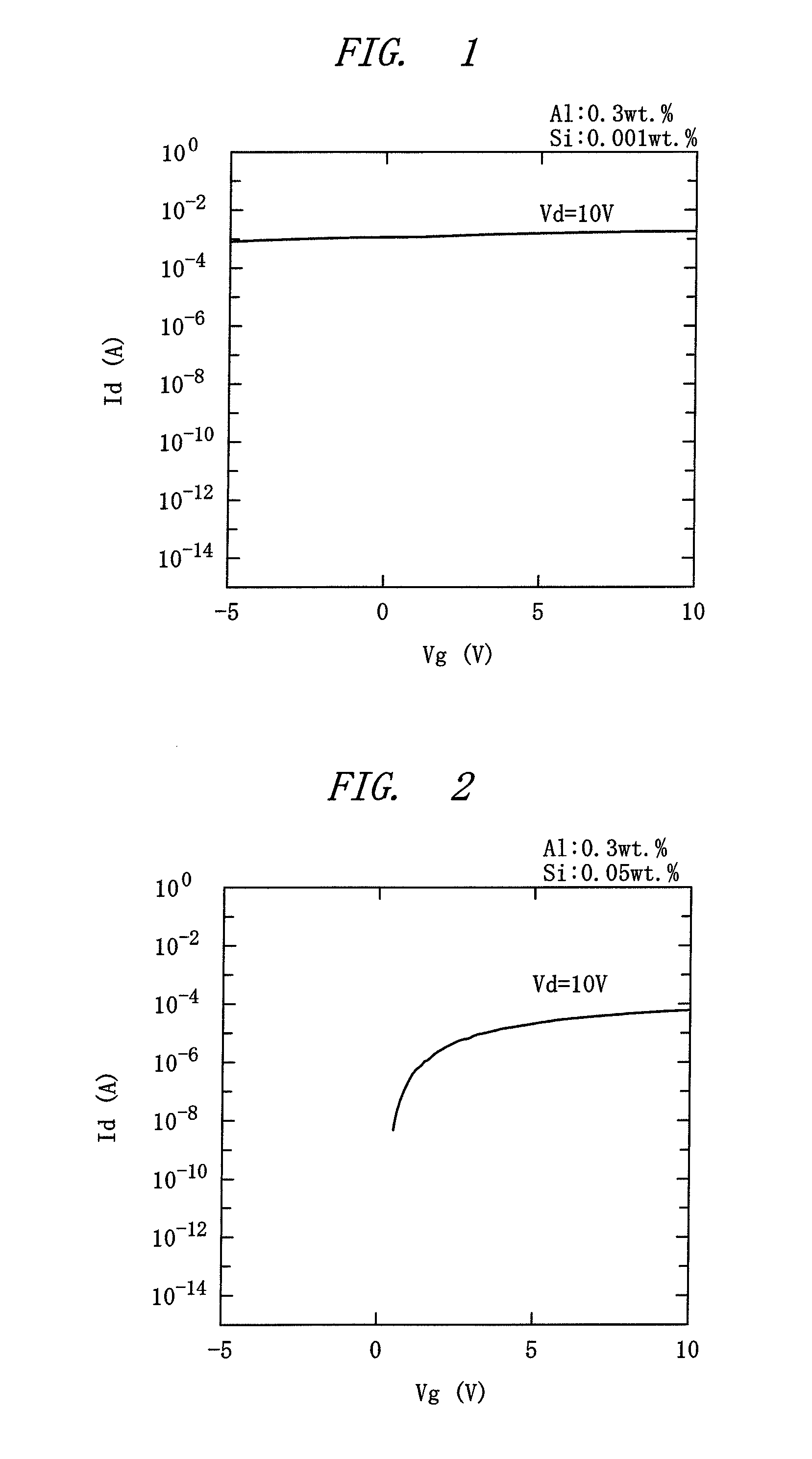
[0043]FIG. 1 is a graph illustrating current (Id)-voltage (Vg) characteristics of a thin-film transistor in which, Al (the group III element) is purposely added to a raw material in a manufacturing step for a ZTO target to lower a purity of the ZTO target down to 2 N level, and a ZTO film formed with using the ZTO target is adopted for the channel layer.

[0044]A normal thin-film transistor has to show current-volta...

second embodiment

[0076](Second Embodiment)

[0077]In the above-described first embodiment, the case that the invention of the present application is adopted for the ZTO target has been described. In a second embodiment, a case that the invention of the present application is adopted for an indium zinc tin oxide (IZTO) target is described.

[0078]First, an example of a method of manufacturing an IZTO layer according to the second embodiment is described. The IZTO layer is formed by an electron-beam deposition method with using the IZTO target. FIG. 9 illustrates a schematic diagram of an electron-beam deposition apparatus according to the second embodiment.

[0079]In the case of the target with using the beam, a relatively-high-density target is not required, and a relatively-large-shape is not required, either, from a point of view in a beam diameter. A basic manufacturing method for the IZTO target is the same as that of the above-described first embodiment. However, in the case of not requiring the high...


PUM

PropertyMeasurementUnit
resistivityaaaaaaaaaa
band gapaaaaaaaaaa
voltageaaaaaaaaaa

Abstract

A technique capable of forming an oxide semiconductor target with a high quality in a low cost is provided. In a step of manufacturing zinc tin oxide (ZTO target) used in manufacturing an oxide semiconductor forming a channel layer of a thin-film transistor, by purposely adding the group IV element (C, Si, or Ge) or the group V element (N, P, or As) to a raw material, excessive carriers caused by the group III element (Al) mixed in the step of manufacturing the ZTO target are suppressed, and a thin-film transistor having good current (Id)-voltage (Vg) characteristics is achieved.

Description

CROSS-REFERENCE TO RELATED APPLICATION[0001]The present application claims priority from Japanese Patent Application No. 2010-171817 filed on Jul. 30, 2010, the content of which is hereby incorporated by reference into this application.TECHNICAL FIELD OF THE INVENTION[0002]The present invention relates to an oxide semiconductor target and a method of manufacturing an oxide semiconductor film with using the oxide semiconductor target. More particularly, the present invention relates to a technique effectively applied to an oxide semiconductor target formed of a sintered oxide mainly made of zinc oxide and tin oxide, and a method of manufacturing an oxide semiconductor film with using the oxide semiconductor target by a sputtering method or a deposition method.BACKGROUND OF THE INVENTION[0003]In recent years, a display device has been developed from a display device with using a cathode-ray tube to a flat-type display device called a flat panel display (FPD) such as a liquid crystal d...

Claims


Application Information

Patent Timeline
Patent Type & Authority Patents(United States)
IPC IPC(8): H01B1/08C23C14/08C23C14/34H01L21/02
CPCH01L21/02631C23C14/086C23C14/3414H01L21/02554H01L21/02565H01L21/02573
Inventor UCHIYAMA, HIROYUKIWAKANA, HIRONORI
Owner HITACHI METALS LTD
Learn More