Multicolor photonic crystal laser array

a photonic crystal and laser array technology, applied in lasers, laser optical resonators, semiconductor lasers, etc., can solve the problems that current surface-emitting lasers and conventional edge-emitting lasers that require abrupt changes in semiconductor bandgaps or cavity lengths are not viable solutions for this requirement, and achieve low thresholds and high yield.

Active Publication Date: 2015-04-28
NAT TECH & ENG SOLUTIONS OF SANDIA LLC
View PDF2 Cites 3 Cited by
  • Summary
  • Abstract
  • Description
  • Claims
  • Application Information

AI Technical Summary

Benefits of technology

[0007]As an example of the invention, a surface emitting, single-mode 2DPC optically pumped laser emitting in the blue-violet spectral region was demonstrated to have a remarkable 60 nm of tuning (or 16% of the nominal centre wavelength), determined purely by the photonic crystal geometry. This wide tuning in emission wavelength was achieved by employing two gain sections (GaN / InGaN MQWs and InGaN underlayer) covering different wavelength bands with broad gain bandwidth in conjunction with careful 2DPC design to select the lasing wavelength. Electron beam lithography was utilized to pattern the InGaN / GaN nanowire hexagonal lattice based 2DPC combined with a novel top-down nanofabrication method. The exquisite control enabled by the two-step, top-down etch process enables excellent quality nanowire arrays with controlled geometries and very high yield. Normal direction lasing emission, with relatively low thresholds, was achieved by using the slow group velocity modes near the Γ point of the 2DPCs at higher bands. This approach can be used to include additional gain sections in order to cover the entire visible spectrum. The fabrication approach can also be appropriately modified to utilize doped structures to create electrically injected devices. The invention enables solid-state lighting devices and displays fabricated using III-nitride 2DPC nanowire lasers to have dynamic colour tuning over a larger colour gamut.

Problems solved by technology

Conventional edge-emitting lasers and current surface-emitting lasers that require abrupt changes in semiconductor bandgaps or cavity length are not a viable solution for this requirement.

Method used


Image

  • Multicolor photonic crystal laser array
  • Multicolor photonic crystal laser array
  • Multicolor photonic crystal laser array

Examples


Embodiment Construction

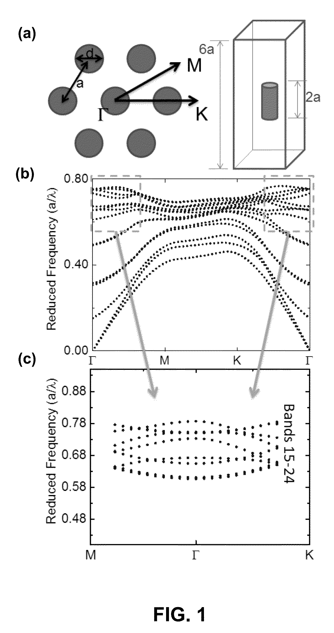
[0018]Sufficiently broadened gain spectra are necessary in order to fabricate an array of lasers that span a large spectral bandwidth. One way of obtaining a broad enough gain spectrum is by choosing an active material with gain that is sufficiently inhomogeneously broadened. However, these broadened gain spectra are often viewed as detrimental due to the reduced peak gain, resulting in an increase of the laser threshold. The rich dispersion characteristics of photonic crystals (PCs) provide an elegant solution to this problem. Photonic crystals are composed of periodic dielectric nanostructures that affect the propagation of electromagnetic waves by defining allowed and forbidden optical bands. Therefore, PCs contain regularly repeating regions of high and low dielectric constant. The periodicity of the photonic crystal structure is less than the wavelength of the electromagnetic waves that are to be diffracted.

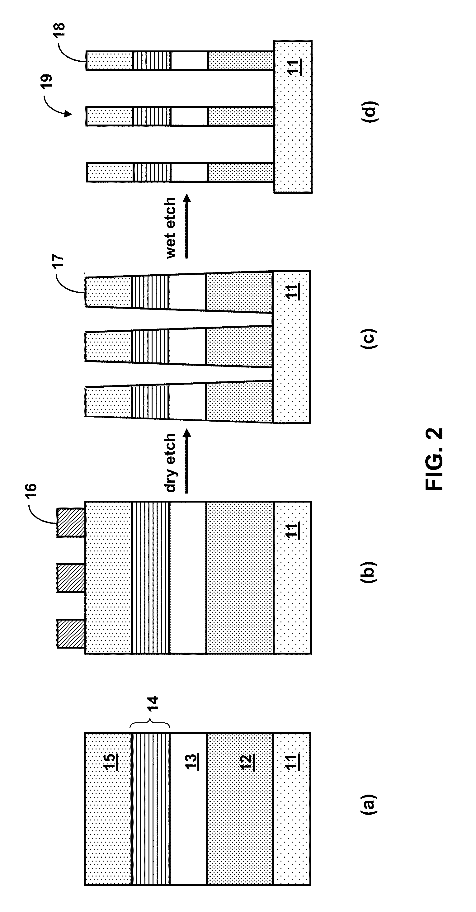
[0019]Photonic crystal lasers comprise active gain region nanostructure...


PUM


Abstract

A multicolor photonic crystal laser array comprises pixels of monolithically grown gain sections each with a different emission center wavelength. As an example, two-dimensional surface-emitting photonic crystal lasers comprising broad gain-bandwidth III-nitride multiple quantum well axial heterostructures were fabricated using a novel top-down nanowire fabrication method. Single-mode lasing was obtained in the blue-violet spectral region with 60 nm of tuning (or 16% of the nominal center wavelength) that was determined purely by the photonic crystal geometry. This approach can be extended to cover the entire visible spectrum.

Description

CROSS-REFERENCE TO RELATED APPLICATION[0001]This application claims the benefit of U.S. Provisional Application No. 61 / 760,418, filed Feb. 4, 2013, which is incorporated herein by reference.STATEMENT OF GOVERNMENT INTEREST[0002]This invention was made with Government support under contract no. DE-AC04-94AL85000 awarded by the U.S. Department of Energy to Sandia Corporation. The Government has certain rights in the invention.FIELD OF THE INVENTION[0003]The present invention relates to vertically emitting laser arrays and, in particular, to a multicolor photonic crystal laser array that can be used for lighting and displays.BACKGROUND OF THE INVENTION[0004]Surface-emitting photonic crystal (PC) lasers are promising light sources for the next-generation of compact and efficient light emitters used in data storage, biomedical applications, solid-state lighting and display technologies. See M. Ikeda and S. Uchida, physica status solidi (a) 194, 407 (2002); H. M. Shapiro, Practical Flow C...

Claims


Application Information

Patent Timeline
Patent Type & Authority Patents(United States)
IPC IPC(8): H01S5/00H01S5/183H01S5/185H01S5/187H01S5/34H01S5/343H01S5/42
CPCH01S5/187H01S5/18H01S5/18319H01S5/10H01S5/105H01S5/1228H01S5/341H01S5/3428H01S5/34333H01S5/42H01S5/11H01S5/185
Inventor WRIGHT, JEREMY B.BRENER, IGALSUBRAMANIA, GANAPATHI S.WANG, GEORGE T.LI, QIMING
Owner NAT TECH & ENG SOLUTIONS OF SANDIA LLC
Why Eureka
Try Eureka