Flash memory for code and data storage

a flash memory and data storage technology, applied in the field of flash memory, can solve the problems of inability to optimize random access write, inability to write on a block basis, and the additional complexity and cost of managing both types of memory with their own interfaces, and achieves the effect of high capacity and easy and economical integration into the system

Active Publication Date: 2015-04-28
WINBOND ELECTRONICS CORP
View PDF20 Cites 5 Cited by
  • Summary
  • Abstract
  • Description
  • Claims
  • Application Information

AI Technical Summary

Problems solved by technology

While both serial and parallel flash memory interfaces are in use, serial flash is becoming increasingly popular due to cost, space and pin-count advantages.
NAND-type flash memory is written page-by-page, which is very suitable for sequential writes but not optimal for random access writes.
Moreover, while reading and programming is performed page-by-page, erasure can only be performed on a block basis.
Unfortunately, the additional complexity and cost to these systems of managing both types of memory with their own interfaces can be significant.
Moreover, to support two different interfaces, the controller requires more pins which increase the cost.
However, DiskOnChip is expensive.

Method used


Image

  • Flash memory for code and data storage
  • Flash memory for code and data storage
  • Flash memory for code and data storage

Examples


Embodiment Construction

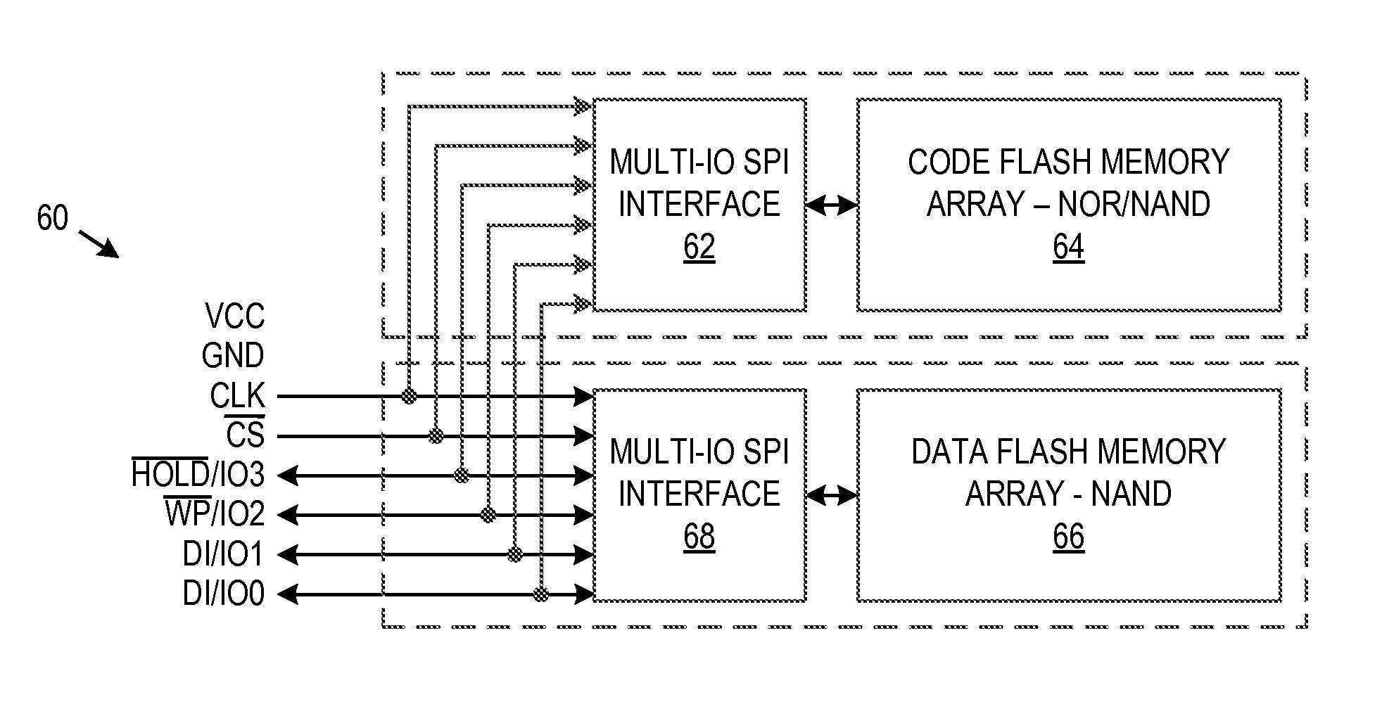
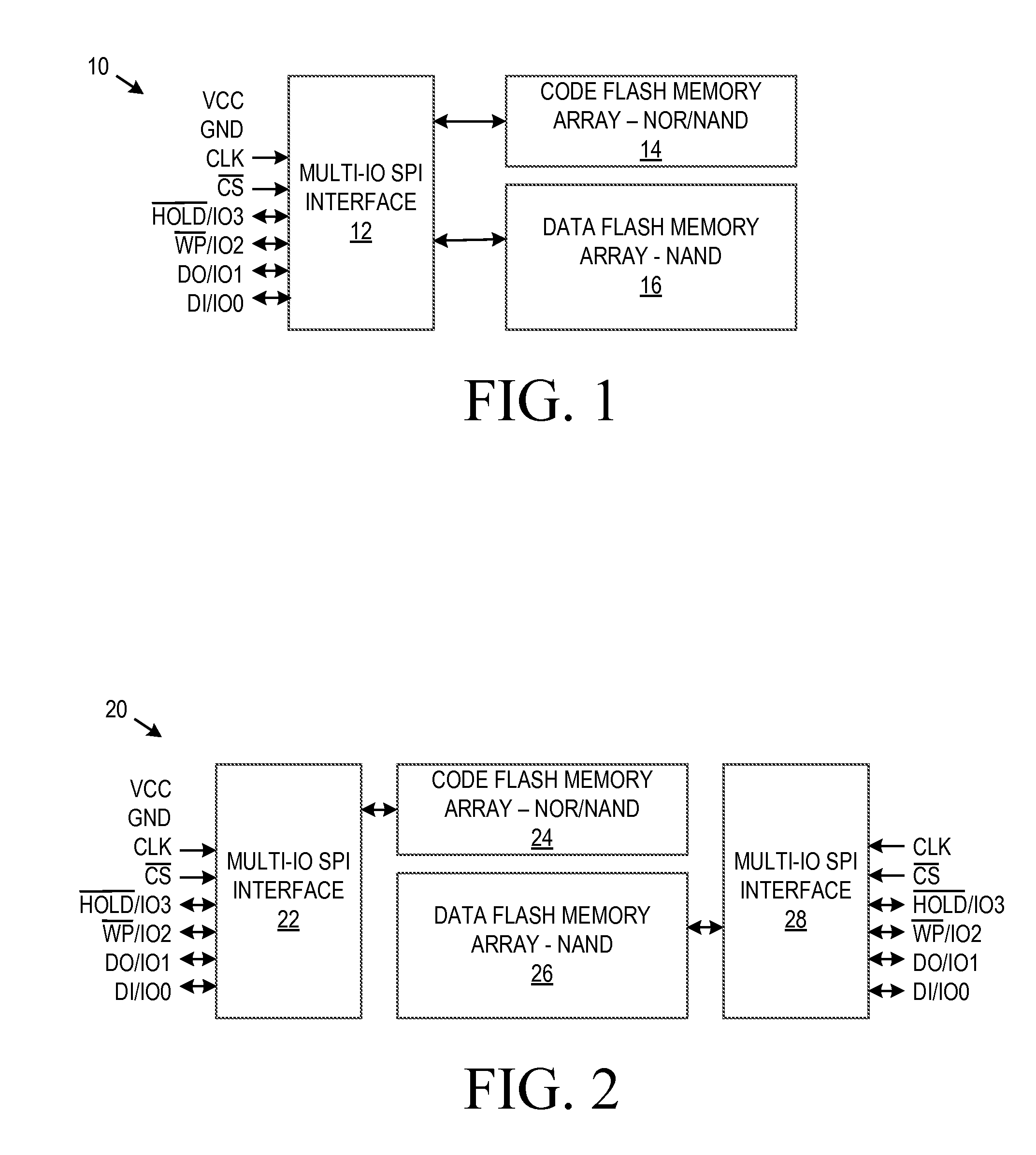
[0041]FIG. 1 is a schematic block diagram of an illustrative implementation of a high speed flash memory 10 for code and data storage. The memory 10 includes a code memory array 14 having fast read access and suitability for execute in place (“XIP”), a data memory array 16 having the characteristics of low bit cost and high density storage, and a multi-IO interface 12 to provide configurable and low pin count serial access to both the code and data. The memory 10 may be implemented in a single chip package or multi-chip package solution, the single chip package solution being less expensive.

[0042]The multi-IO interface 12 illustratively a multi-IO SPI (Serial Peripheral Interface) interface, although other types of configurable serial interfaces may be used as well. The interface 12 shown in FIG. 1 is a six pin implementation (exclusive of power and ground) configurable as single SPI, dual SPI, and quad SPI. The pins provided are power VCC, ground GND, chip select CS, clock CLK, con...


PUM


Abstract

A flash memory for code and data storage includes a code memory array having fast read access and suitability for execute in place, a data memory array having the characteristics of low bit cost and high density storage, and a suitable interface to provide access to both the code and data. The code memory array may be a NOR array or a performance-enhanced NAND array. The memory may be implemented in a single chip package or multi-chip package solution.

Description

CROSS-REFERENCE TO RELATED APPLICATIONS[0001]This application claims the benefit of U.S. Provisional Patent Application Ser. No. 61 / 389,253 filed Oct. 3, 2010, which hereby is incorporated herein in its entirety by reference thereto.BACKGROUND OF THE INVENTION[0002]1. Field of the Invention[0003]The present invention relates to flash memory, and more particularly to flash memory for both code and data storage.[0004]2. Description of Related Art[0005]Flash memory is a non-volatile computer storage technology that is electrically erasable typically in large blocks, which gives it a speed advantage over small-block EEPROM technology. Flash memory stores digital data in an array of memory cells made from charge-storing floating-gate transistors, which may be single-level or multi-level. The array may be NOR-type or NAND-type. While both serial and parallel flash memory interfaces are in use, serial flash is becoming increasingly popular due to cost, space and pin-count advantages.[0006]...

Claims


Application Information

Patent Timeline
Patent Type & Authority Patents(United States)
IPC IPC(8): G06F12/02G11C11/00G11C16/04
CPCG06F12/0246G11C11/005G06F2212/7208G11C16/0416G11C16/0483G11C2216/30G06F3/0608G06F3/061G06F3/0658G06F3/0688
Inventor PARK, EUNGJOONJIGOUR, ROBIN JOHNPARK, JOOWEONYANO, MASARU
Owner WINBOND ELECTRONICS CORP
Why Eureka
Try Eureka