Measuring apparatus and plasma processing apparatus

a technology of measuring apparatus and plasma processing, which is applied in the direction of optical radiation measurement, instruments, semiconductor/solid-state device testing/measurement, etc., can solve the problems of inability to implement high-resolution spectrum when using infrared rays, and the physical inability to increase the wavelength resolution power to be higher than the number of elements, so as to increase the thickness range of measurable examination targets and increase wavelength resolution power.

Active Publication Date: 2015-06-30
TOKYO ELECTRON LTD
View PDF9 Cites 4 Cited by
  • Summary
  • Abstract
  • Description
  • Claims
  • Application Information

AI Technical Summary

Benefits of technology

[0012]The present invention provides a measuring apparatus and a plasma processing apparatus, capable of increasing a thickness range of a measurable examination target by increasing a wavelength resolution power.

Problems solved by technology

However, in the spectroscope using a CCD array or a photodiode array, a wavelength resolution power or the sampling number in wavelength domain is determined according to the number of elements, and thus it is physically impossible to increase the wavelength resolution power to be higher than the number of elements.
In addition, the wavelength resolution power is limited to 3648 in a visible region and to 512 to 1024 in an infrared region, and thus the wavelength resolution power cannot be increased more than the above limitations.
Thus, spectrum of a high resolution cannot be implemented when using, in particular, infrared rays, compared with visible rays.
On the other hand, there is a correlation between the wavelength resolution power and a thickness of an examination target that can be measured, and the lower the wavelength resolution power becomes, the more the thickness of the measurable examination target is limited.
Therefore, up to now, a thickness of the examination target that can be measured by using a general CCD array or a photodiode array is limited to be very thin.
For example, in a plasma processing apparatus, a thickness of a wafer may be measured; however, a thick member having a thickness to a certain degree, such as a focus ring, or the like cannot be measured.

Method used


Image

  • Measuring apparatus and plasma processing apparatus
  • Measuring apparatus and plasma processing apparatus
  • Measuring apparatus and plasma processing apparatus

Examples


Embodiment Construction

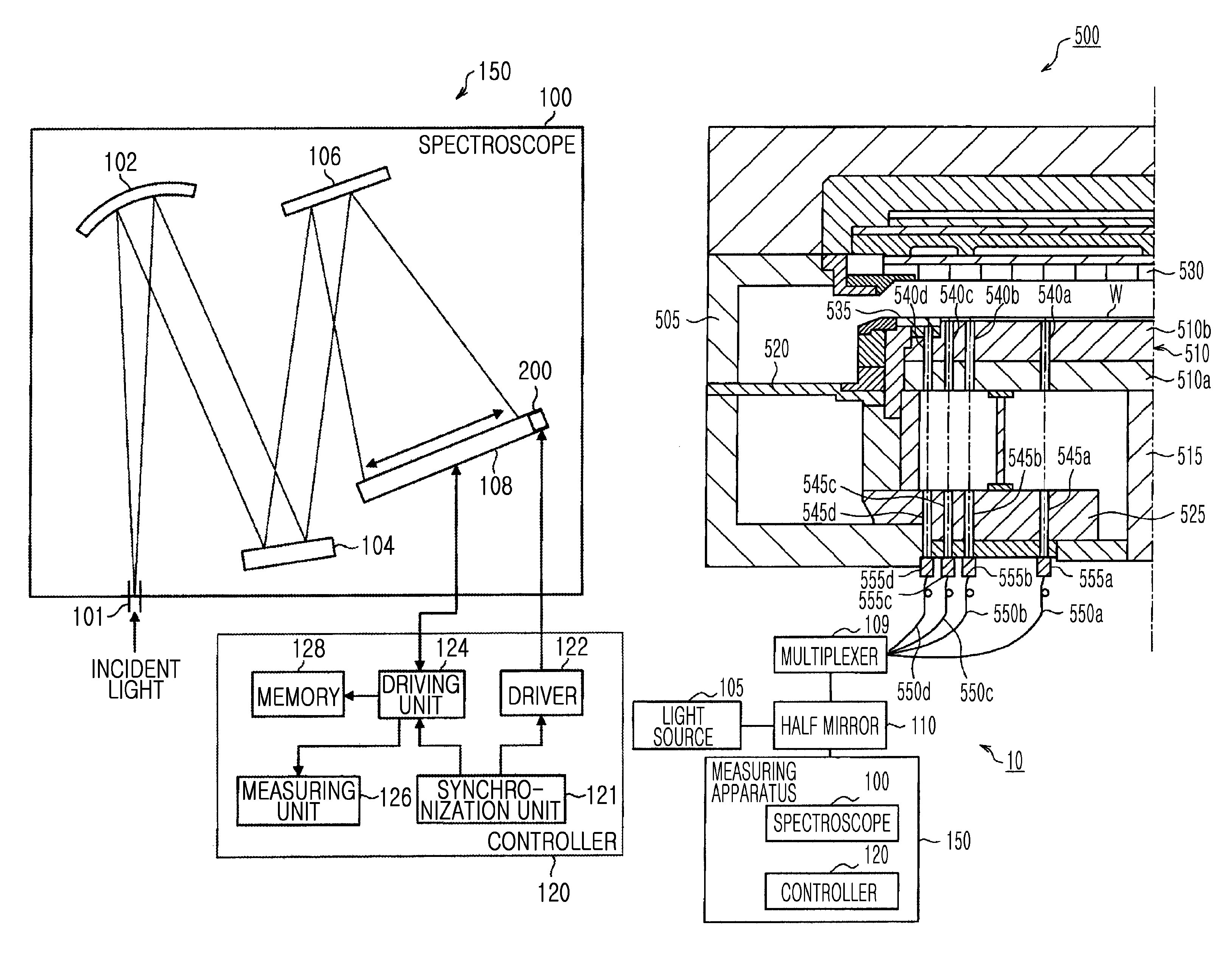
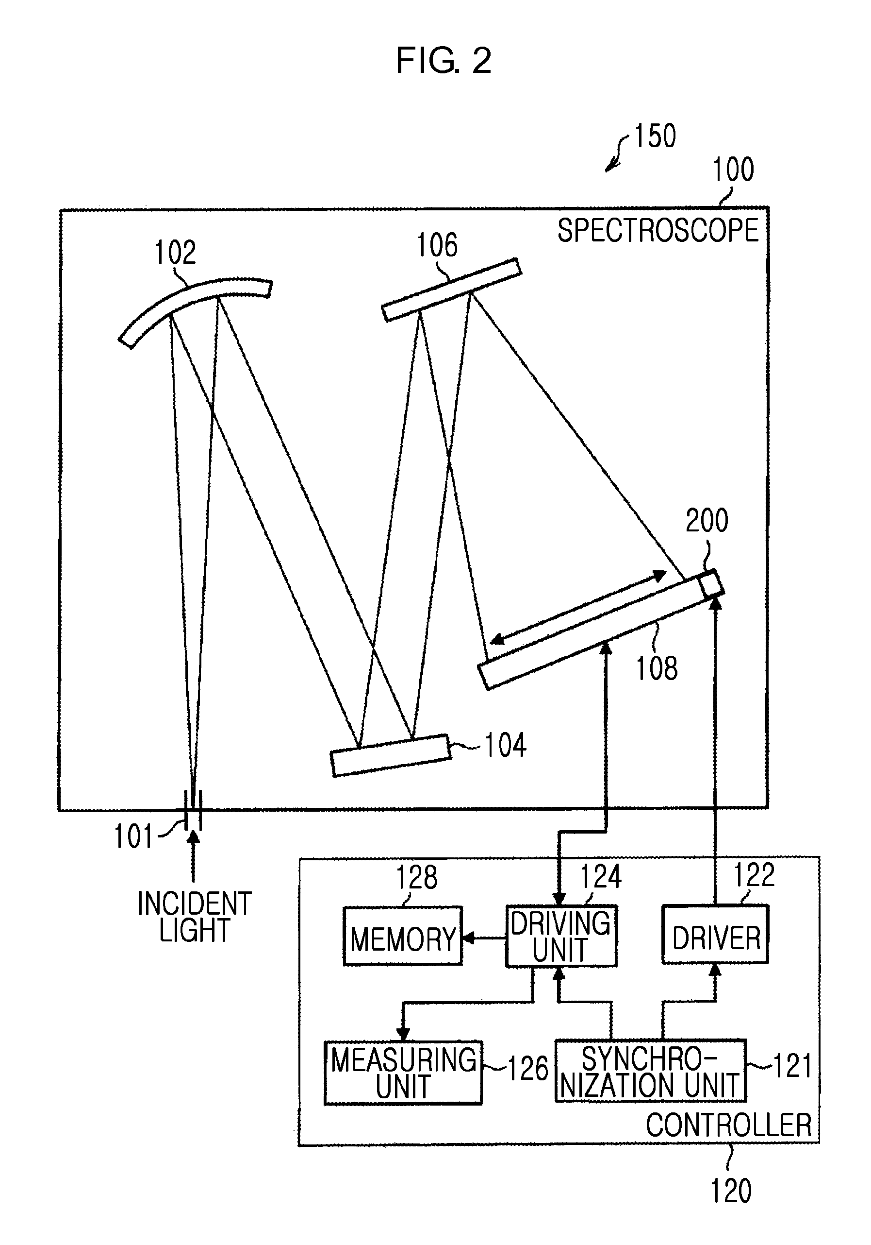
[0026]The attached drawings for illustrating exemplary embodiments of the present invention are referred to in order to gain a sufficient understanding of the present invention, the merits thereof, and the objectives accomplished by the implementation of the present invention. Hereinafter, the present invention will be described in detail by explaining exemplary embodiments of the invention with reference to the attached drawings. Like reference numerals in the drawings denote like elements and a repeated explanation thereof will not be given.

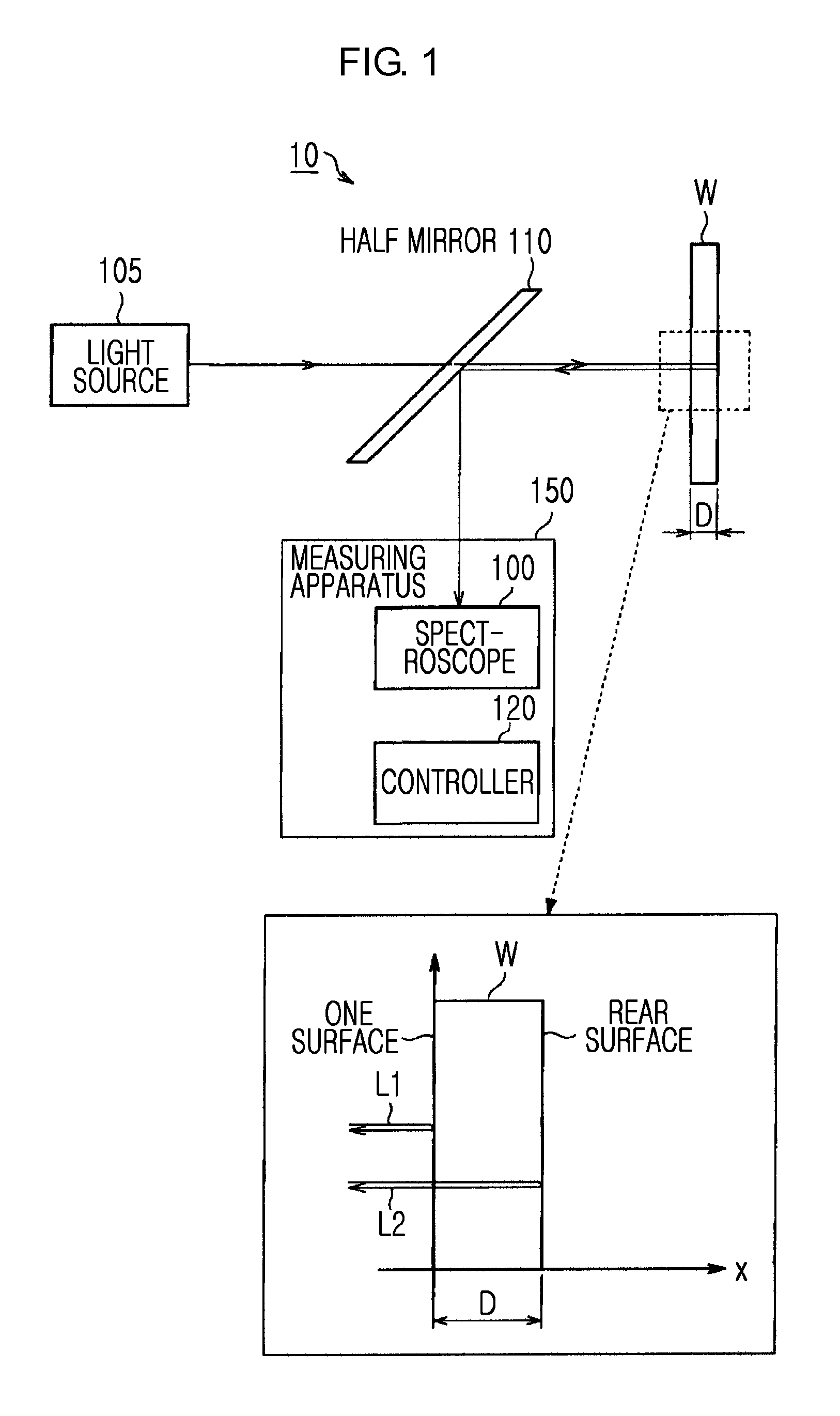
[0027]To begin with, a measuring system using a movable mirror will be described with reference to FIG. 6, as a comparative example with a measuring system according to an embodiment of the present invention. In the measuring system 99 according to the comparative example, a temperature measuring method in consideration of a time domain is provided.

[0028]First, light output from a light source 92 is split into measuring light Ls and reference l...


PUM

PropertyMeasurementUnit
optical path lengthaaaaaaaaaa
wavelength band rangeaaaaaaaaaa
thicknessaaaaaaaaaa

Abstract

Provided a measuring apparatus includes a wavelength dispersion device which dispersed light reflected by one surface of an examination target having a thickness D and light reflected by a rear surface of the examination target, as incident light, a detector in which a plurality of photodetection elements receiving light dispersed by the wavelength dispersion device and detecting a power of the received light in are provided in an array shape, and a piezoelectric device which is attached to the detector to convert an applied voltage into a mechanical power, wherein the detector detects the power of the received light when the detector is shifted by the mechanical power converted by the piezoelectric device as much as d / m, where d is a width of each of the photodetection elements in an array direction and m is an integer equal to or greater than 2.

Description

CROSS-REFERENCE TO RELATED PATENT APPLICATIONS[0001]This application claims the benefit of Japanese Patent Application No. 2011-74979, filed on Mar. 30, 2011, in the Japanese Patent Office, and U.S. Patent Application No. 61 / 537,718 filed on Sep. 22, 2011 in the U.S. Patent and Trademark Office, the disclosure of which is incorporated herein in its entirety by reference.BACKGROUND OF THE INVENTION[0002]1. Field of the Invention[0003]The present invention relates to a measuring apparatus and a plasma processing apparatus, and more particularly, to an apparatus for optically measuring an examination target.[0004]2. Description of the Related Art[0005]When etching or film formation is performed on, for example, a semiconductor wafer (hereinafter, referred to as a wafer), controlling of a temperature of the wafer is relevant to a film forming rate or an etching rate of the wafer, thereby affecting features of a film or a shape of a hole formed in the wafer. Therefore, it is important to...

Claims


Application Information

Patent Timeline
Patent Type & Authority Patents(United States)
IPC IPC(8): C23C16/00G01K5/50G01K11/00H01J37/32C23F1/00H01L21/67
CPCH01L21/67248G01K5/50G01K11/00H01J37/32972H01L22/00
Inventor MATSUDO, TATSUOKIMURA, HIDETOSHI
Owner TOKYO ELECTRON LTD
Why Eureka
Try Eureka