Statistical overlay error prediction for feed forward and feedback correction of overlay errors, root cause analysis and process control

a technology of overlay errors and statistical overlays, applied in the field of statistical overlay errors prediction of feed forward and feedback correction of overlay errors, can solve problems such as overlay errors, adversely affecting integrated circuit performance and wafer yield, and overlay errors that consume a significant fraction of the total overlay budget for critical layers, and achieve accurate prediction corrections

Active Publication Date: 2015-07-21
KLA TENCOR TECH CORP
View PDF4 Cites 36 Cited by
  • Summary
  • Abstract
  • Description
  • Claims
  • Application Information

AI Technical Summary

Benefits of technology

[0009]In at least one embodiment, an overlay prediction system accurately predicts corrections by determining wafer geometry changes based on measurements of the wafer before and after lithography processes, applying a plurality of predictive models and comparing the predictive models to actual overlay errors to determine which predictive model produces the most accurate result. The identified predictive model is then used to predict overlay errors in subsequent wafer fabrication for the same batch of wafers. In another embodiment, a validation wafer is used to verify the identified predictive model.

Problems solved by technology

Lithography overlay and critical dimension uniformity (CDU) are critical parameters in semiconductor manufacturing which can adversely affect integrated circuit performance and wafer yield.
Overlay errors can be caused by lithography scanner tools, mask or reticle, and process induced wafer geometry changes during scan and expose operation or other similar sources.
With shrinking logic and memory device dimensions, overlay errors increasingly consume a significant fraction of the total overlay budget for critical layers.
However these methods suffer from the high complexity of the physical processes.
Furthermore, they impact the wafer geometry that they seek to model and may not be usable to consistently predict reliable scanner corrections to counteract incoming wafer geometry changes.

Method used


Image

  • Statistical overlay error prediction for feed forward and feedback correction of overlay errors, root cause analysis and process control
  • Statistical overlay error prediction for feed forward and feedback correction of overlay errors, root cause analysis and process control
  • Statistical overlay error prediction for feed forward and feedback correction of overlay errors, root cause analysis and process control

Examples


Embodiment Construction

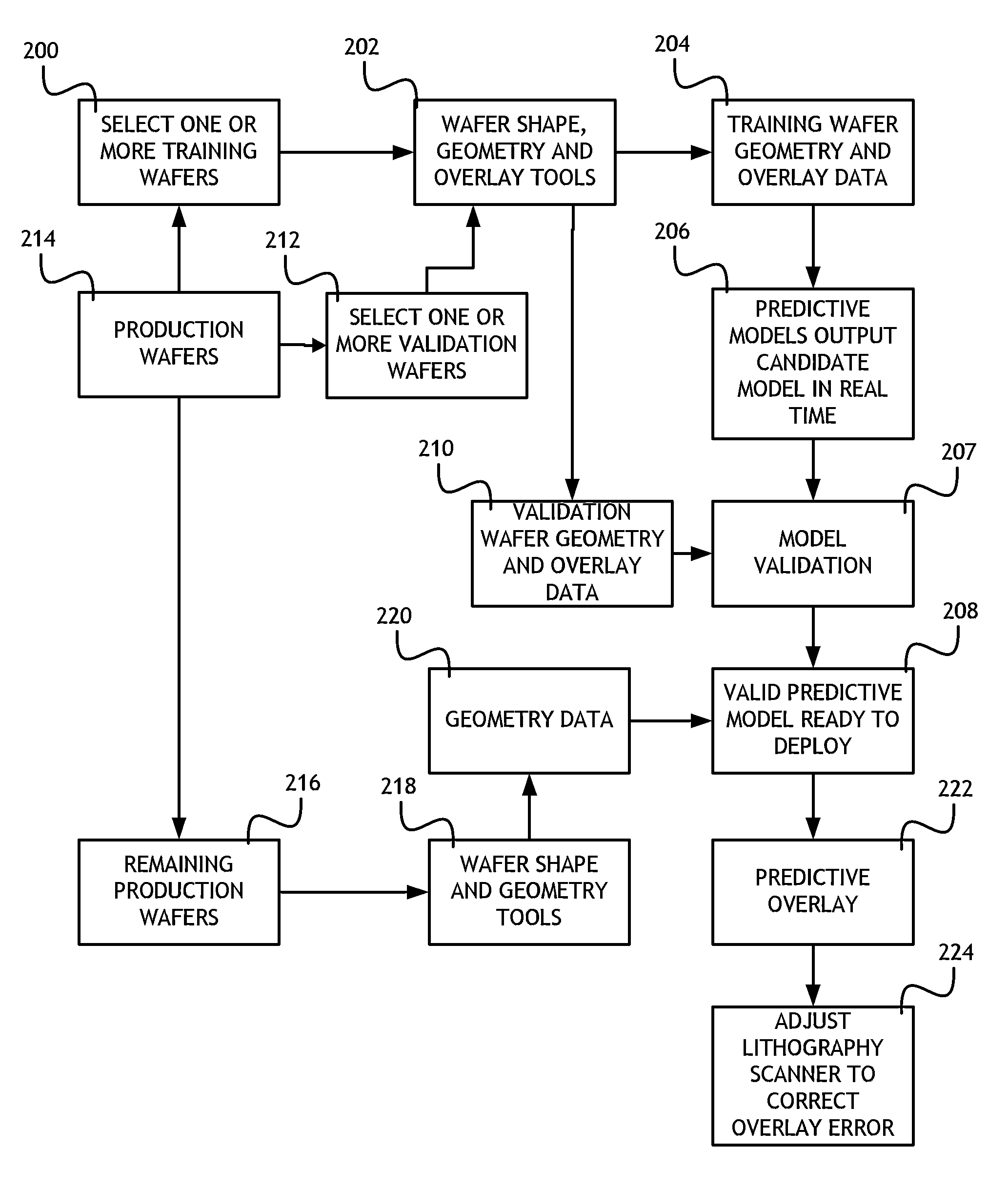
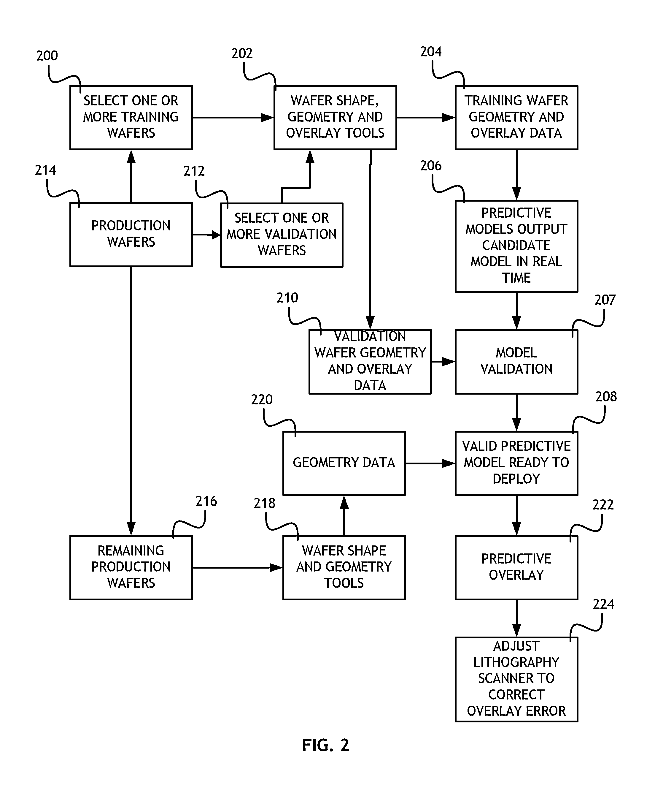
[0016]Reference will now be made in detail to the subject matter disclosed, which is illustrated in the accompanying drawings. The scope of the invention is limited only by the claims; numerous alternatives, modifications and equivalents are encompassed. For the purpose of clarity, technical material that is known in the technical fields related to the embodiments has not been described in detail to avoid unnecessarily obscuring the description.

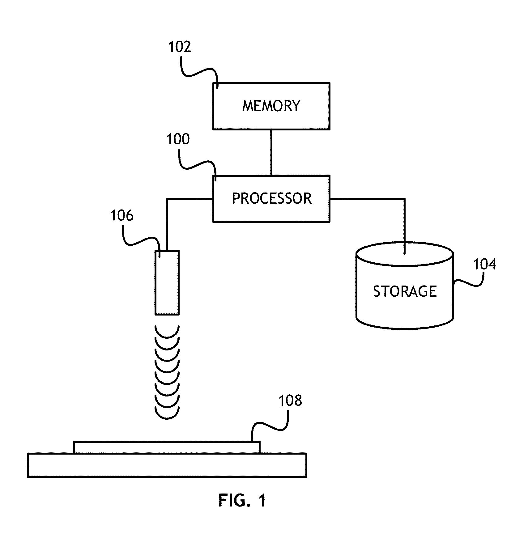
[0017]Referring to FIG. 1, a block diagram of a lithographic computer system useful for implementing at least one embodiment of the present invention is shown. In at least one embodiment of the present invention, a computer system for scanning wafers and determining a predictive model of overlay errors in a wafer fabrication process includes a processor 100, memory 102 connected to the processor 100 for storing and executing computer executable program code and a camera 106 or other wafer scanning device for scanning a wafer 108 geometry and ...


PUM

PropertyMeasurementUnit
flatnessaaaaaaaaaa
thicknessaaaaaaaaaa
critical dimensionaaaaaaaaaa

Abstract

A method to collect data and train, validate and deploy statistical models to predict overlay errors using patterned wafer geometry data and other relevant information includes selecting a training wafer set, measuring at multiple lithography steps and calculating geometry differences, applying a plurality of predictive models to the training wafer geometry differences and comparing predicted overlay to the measured overlay on the training wafer set. The most accurate predictive model is identified and the results fed-forward to the lithography scanner tool which can correct for these effects and reduce overlay errors during the wafer scan-and-expose processes.

Description

PRIORITY[0001]The present application claims the benefit under 35 U.S.C. §119(e) of U.S. Provisional Application Ser. No. 61 / 949,022, filed Mar. 6, 2014, which is incorporated herein by reference.FIELD OF THE INVENTION[0002]The present invention is directed generally toward semiconductor wafer fabrication and more particularly toward error identification and correction methods in fabrication.BACKGROUND OF THE INVENTION[0003]A wafer generally goes through certain processes including deposition, etching, chemical-mechanical polishing (CMP) etc., before it is sent into a lithography scanner for exposure. Overlay errors are measured after the exposure using tools such as TWINSCAN, Archer 500 or some other appropriate device.[0004]Lithography overlay and critical dimension uniformity (CDU) are critical parameters in semiconductor manufacturing which can adversely affect integrated circuit performance and wafer yield. Overlay errors can be caused by lithography scanner tools, mask or reti...

Claims


Application Information

Patent Timeline
Patent Type & Authority Patents(United States)
IPC IPC(8): G06F17/50G03F1/36G03F7/20G03F1/00G06N20/00
CPCG06F17/5081G06F17/5068G03F7/705G03F1/36G03F1/144G06F2217/12G03F7/70633G06F30/398G06F2119/18Y02P90/02G06N20/00G03F7/706G06F30/39G06N5/04
Inventor CHANG, WEIRAO, KRISHNAGUTIERREZ, JOSEPHOLAVARRIA, RAMONMACNAUGHTON, CRAIGAZORDEGAN, AMIRDIGHE, PRASANNASINHA, JAYDEEP
Owner KLA TENCOR TECH CORP
Why Eureka
Try Eureka