Carrier-free land grid array IC chip package and preparation method thereof

a carrier-free, pinless technology, applied in the direction of electrical apparatus, semiconductor devices, semiconductor/solid-state device details, etc., can solve the problems of low production yield of substrates, low cost of ceramic substrates, and long manufacturing cycle, and achieve desirable heat dissipation effects, high yield, and simple and flexible structure

Active Publication Date: 2015-09-15
TIANSHUI HUATIAN TECH
View PDF13 Cites 3 Cited by
  • Summary
  • Abstract
  • Description
  • Claims
  • Application Information

AI Technical Summary

Benefits of technology

[0040]The present invention adopts approximate square-shaped spherical array contacts, thereby having a simple and flexible structure, and achieving a desirable heat-dissipation effect. The cooper L / F has a high yield and high material utilization, and reduces the material cost. The L / F is used to replace the ceramic substrate, the PCB substrate, or the BT substrate, thereby saving the complicated layout design, shortening the designing and manufacturing cycle, accelerating the trial production course, and enabling the product to be early listed to obtain market opportunities.

Problems solved by technology

A ceramic substrate, a Printed Circuit Board (PCB) substrate, or a Bismaleimide Triazine (BT) substrate is generally used in the PGA packaging technology (unclear logical relation), the layout structural design thereof is complicated, and the cost of the ceramic substrate, the PCB substrate, or the BT substrate is high; moreover, the substrate has low production yield, long manufacturing cycle, and poor heat-dissipation effect.

Method used


Image

  • Carrier-free land grid array IC chip package and preparation method thereof
  • Carrier-free land grid array IC chip package and preparation method thereof
  • Carrier-free land grid array IC chip package and preparation method thereof

Examples


embodiment 1

[0123

[0124]Single-Chip Packaging

[0125]1. Grinding and Sawing

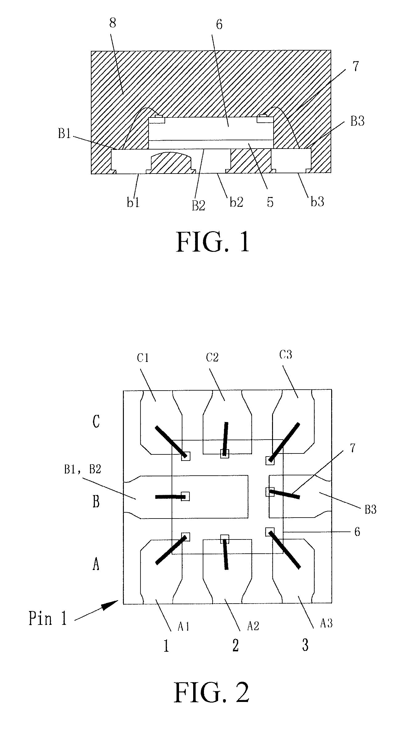
[0126]First a wafer is ground to the thickness of 150 μm, cleaned and dried, and then an adhesive film sheet is adhered at the back; a grinding adhesive film is removed; then the wafer adhered with the adhesive film sheet is sawed into single chips, where only the adhesive film sheet layer is cut thoroughly without hurting a protective layer.

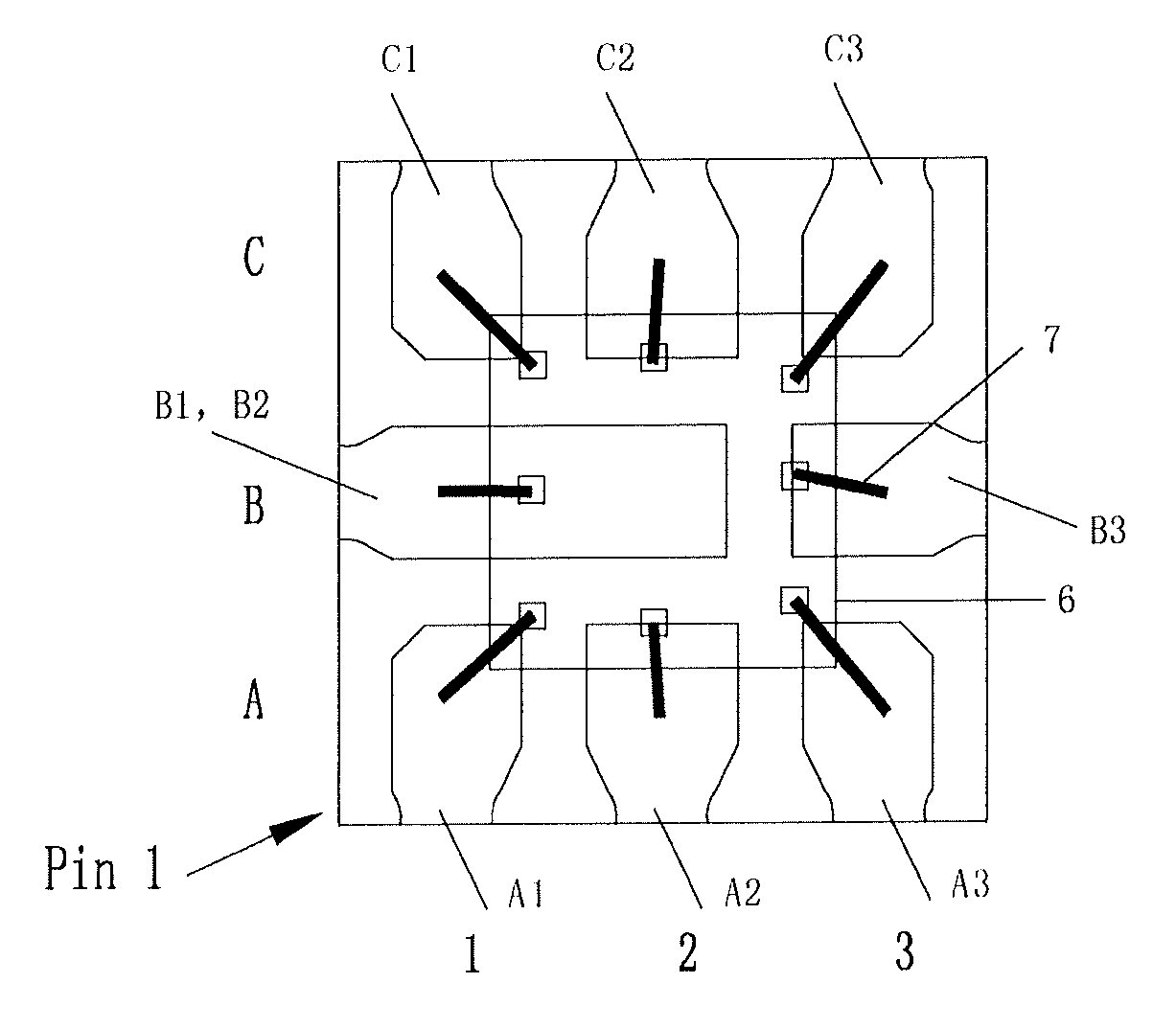
[0127]2. Die Bonding

[0128]An NLGA9L-dedicated frame and an adhesive film sheet are used. On a dedicated die bonder, the L / F is automatically delivered to a track of the die bonder, and the chip is automatically placed at edges of the inner pins B1 and B2 as well as several other inner pins B3, A1, A2, A3, C1, C2, and C3. For the typical three-row pins, because the NLGA frame is carrier-free, the chip with the adhesive film sheet is adhered to edges of the dual pins (for example, NLGA9L, B1, B2, B3) at the row B and several other pins (for example, NLGA9L, A1, A2, A3, C1, C2, C3), and is...

embodiment 2

[0147

[0148]Dual-chip Stacked Packaging

[0149]The grinding, sawing, marking, and cutting in the dual-chip stacked packaging are the same as those in single-chip packaging; matrix gold-plated contacts are used, and electroplating is not adopted.

[0150]1. Grinding and Sawing

[0151]First a wafer at a lower layer is ground to the thickness of 200 μm, a wafer at an upper layer is ground to the thickness of 100 μm; the wafers are cleaned and dried, and then an adhesive film sheet is adhered at the back; a grinding adhesive film is removed. Then the wafer adhered with the adhesive film sheet is sawed into single chips, where a sawing depth parameter is adjusted according to a sum of the thickness of the ground wafer and the adhesive film thickness the adhesive film sheet, only the adhesive film sheet layer is cut thoroughly without hurting a protective layer.

[0152]2. Die Bonding

[0153]The chip is automatically set at a position of the corresponding L / F inner pin on a dedicated die bonder of the...

embodiment 3

[0172

[0173]Multi-Chip Packaging

[0174]The grinding, sawing, marking, and cutting in the multi-chip packaging are the same as those in single-chip packaging; a matrix L / F uses gold-plated contacts, and electroplating is not required.

[0175]1. Grinding and Sawing

[0176]The same as those in Embodiment 1.

[0177]2. Die Bonding

[0178]The chip is automatically set at a position of the corresponding L / F inner pin on a dedicated die bonder of the adhesive film sheet, and is heated; then the IC chip 6 is adhered to edges of the inner pins at the middle row and several other inner pins. For the typical four-row pins, because the NLGA frame is carrier-free, the IC chip 6 with the adhesive film sheet is adhered to the pins (for example, NLGA16L, B2, B3, C2 and C3) at the rows B and C, and the IC chip 9 with the adhesive film sheet is adhered to edges of the pins B4 and C4.

[0179]3. Wiring Bonding

[0180]Because the IC chip 6 is adhered to the inner pins, the pad on the IC chip 6 is close to the inner pi...


PUM


Abstract

A carrier-free land grid array (LGA) Integrated Circuit (IC) chip package and a preparation method thereof are provided. The IC chip package includes: an inner pin, an IC chip, a pad, a bonding wire, and a mold cap. The inner pin is designed to be a multi-row matrix form at a front side of the package, and is designed to be an exposed multi-row approximate square-shaped circular gold-plated contacts at a back side; the IC chip is provided on the inner pin, the inner pin is adhered to the IC chip with an adhesive film sheet, the pad on the IC chip is connected to the inner pin by the bonding wire, and the mold cap encircles the adhesive film sheet, the IC chip, the bonding wire, and edges of the inner pin, so as to form a whole circuit. The present invention adopts approximate square-shaped spherical array contacts, thereby having a simple and flexible structure, and achieving a desirable heat-dissipation effect. A cooper lead frame (L/F) has a high yield, and reduces the material cost. The L/F is used to replace a ceramic substrate, PCB substrate, or BT substrate, thereby saving the complicated layout design, shortening the designing and manufacturing cycle, accelerating the trial production course, and enabling the product to be early listed to obtain market opportunities.

Description

BACKGROUND OF THE INVENTION[0001]1. Field of Invention[0002]The present invention belongs to the field of manufacturing technologies of electronic information automation devices, relates to an Integrated Circuit (IC) chip package, and more particularly to a carrier-free pinless land grid array (LGA) IC chip package; the present invention further relates to a preparation method of the package.[0003]2. Related Art[0004]Land Grid Array (LGA) package is fine-pitch chip-scale package based on a laminated substrate. The LGA replaces the old Pin Grid Array (PGA) through the metal-contact packaging technology, and realizes a progressive technological revolution. A ceramic substrate, a Printed Circuit Board (PCB) substrate, or a Bismaleimide Triazine (BT) substrate is generally used in the PGA packaging technology (unclear logical relation), the layout structural design thereof is complicated, and the cost of the ceramic substrate, the PCB substrate, or the BT substrate is high; moreover, th...

Claims


Application Information

Patent Timeline
Patent Type & Authority Patents(United States)
IPC IPC(8): H01L23/00H01L23/495H01L23/31
CPCH01L24/05H01L23/4951H01L23/49541H01L23/49548H01L23/49575H01L24/03H01L24/97H01L23/3107H01L24/32H01L24/48H01L24/49H01L24/73H01L24/85H01L24/92H01L2223/54486H01L2224/04042H01L2224/2919H01L2224/32145H01L2224/32245H01L2224/48091H01L2224/48137H01L2224/48145H01L2224/48247H01L2224/49171H01L2224/73265H01L2224/85444H01L2224/92247H01L2224/97H01L2924/15747H01L2924/00014H01L2924/00012H01L2924/00H01L2224/83H01L2224/85H01L2924/15787H01L2924/181H01L2924/12042H01L2924/14H01L2224/05554H01L2924/18301H01L2224/45099H01L2224/45015H01L2924/207
Inventor GUO, XIAOWEIHE, WENHAIMU, WEIWANG, XINJUN
Owner TIANSHUI HUATIAN TECH
Why Eureka
Try Eureka