Semiconductor wafer comprising gallium nitride layer having one or more silicon nitride interlayer therein

Active Publication Date: 2015-09-22
INTELLEC
View PDF11 Cites 7 Cited by
  • Summary
  • Abstract
  • Description
  • Claims
  • Application Information

AI Technical Summary

Benefits of technology

[0011]a first GaN layer having one or more SiNx interlayers therein; and
[0012]wherein in the first GaN layer at least one SiNx interlayer h

Problems solved by technology

Common defects in LEDs, for example, include threading (edge or screw type) dislocations which lead to a reduced luminescent efficiency in the final product.
These defects reduce the inte

Method used


Image

  • Semiconductor wafer comprising gallium nitride layer having one or more silicon nitride interlayer therein
  • Semiconductor wafer comprising gallium nitride layer having one or more silicon nitride interlayer therein
  • Semiconductor wafer comprising gallium nitride layer having one or more silicon nitride interlayer therein

Examples


Example

Example 1

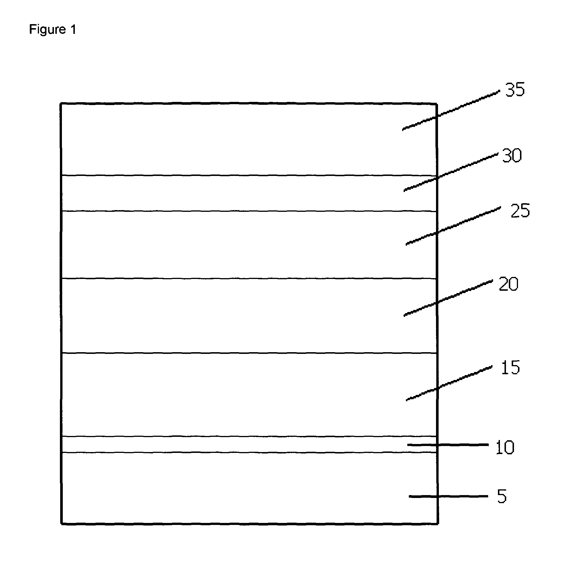
[0066]In this embodiment GaN structures are grown on either 2-inch or 6-inch Si (111) substrates 5 by metalorganic vapour phase epitaxy (MOVPE) in a 6×2″ Aixtron CCS reactor using a 6×2″ or 1×6″ susceptor. Trimethylgallium (TMG), trimethylaluminium (TMA) and trimethylindium (TMI) were used as group-III precursors, while ammonia was used as the nitrogen source. Silane (SiH4) and cyclopentadienyl magnesium (Cp2Mg) are used as the sources of n-type and p type dopants, respectively.

[0067]A flat, crack-free and uniform GaN-based LED structure was grown on 6-inch Si (111) substrate 5 by metal-organic vapour phase epitaxy (MOVPE). The as-supplied Si (111) substrates 5 were first annealed in the reactor to remove the native oxide layer.

[0068]This was followed by the growth of an AlN nucleation layer 10 which prevents Ga from reacting with the Si substrate. An AlGaN buffer layer 15 was then grown to control the stress. The AlN nucleation layer 10 and graded AlGaN buffer layer 15 wer...

Example

Example 2

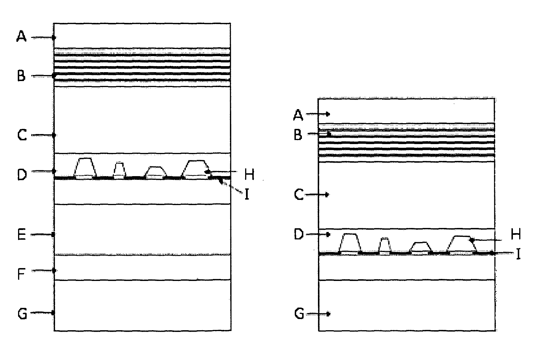
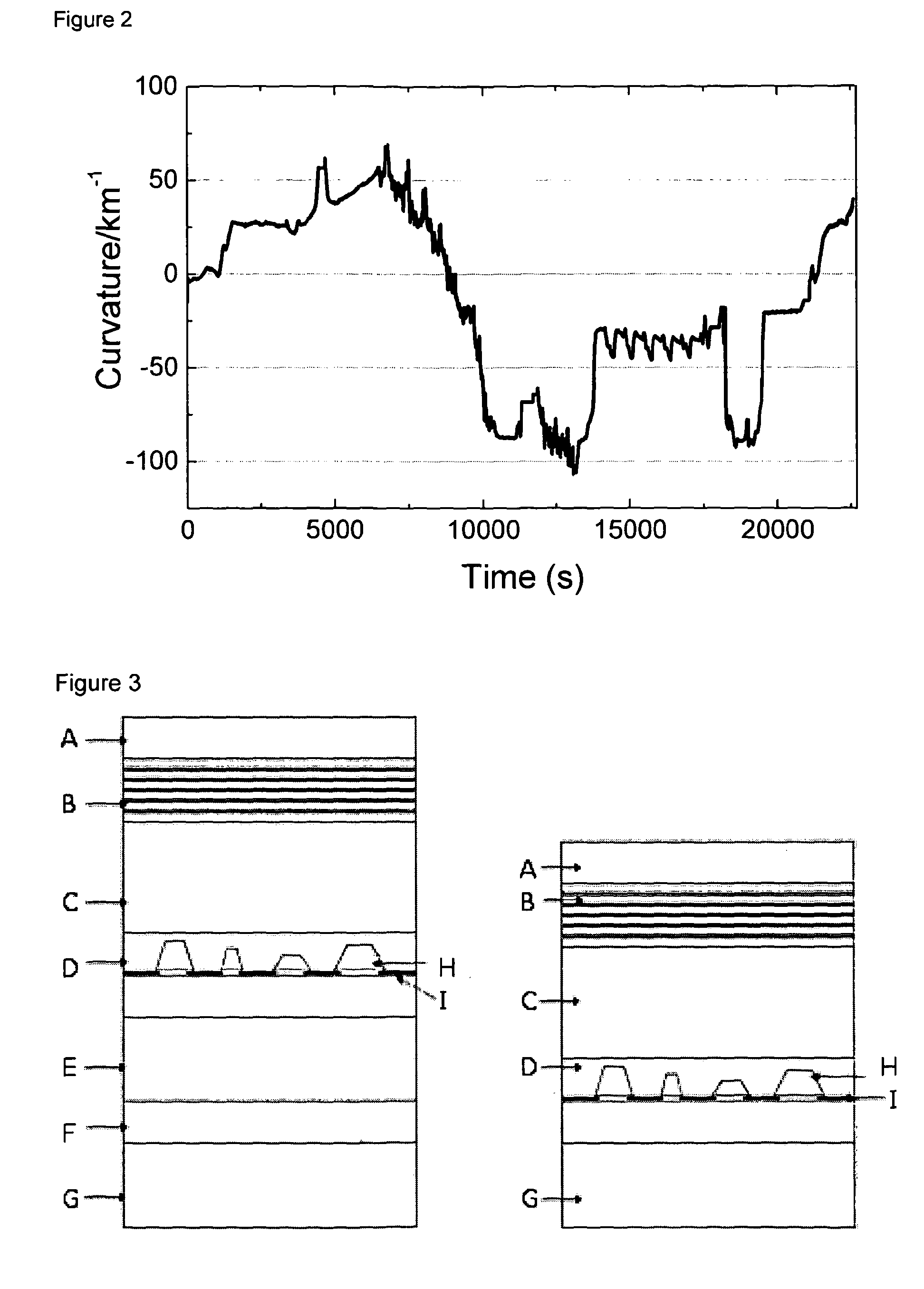
[0076]A commercially available Epicurve®TT sensor (Laytec GmbH) was used to give emissivity-corrected real-time temperature and wafer curvature measurement and an Argus (Aixtron) in-situ temperature profiler was installed on top of the reactor to provide a complete temperature map of the wafer. FIG. 2 shows a trace of the curvature of the wafer during the manufacturing process for a wafer.

[0077]As can be seen in FIG. 2, the curvature of the wafers varies throughout the process.

[0078]Between 1000s and 3000s the substrate was annealed and plateaued at 25 / km. Then a 200 nm AlN nucleation layer was formed which increased the concave form of the wafer. At 7500s the AlGaN buffer layer was formed, and then a GaN layer containing a single interlayer to a total thickness of 1.3 μm. At 12500 a Si-doped GaN layer was formed. Between 14000s and 18000s InGaN—GaN multi quantum wells (MQW) were formed before the wafer composite was allowed to cool. During cooling the curvature dropped fro...

Example

Example 3

[0087]A graded AlGaN buffer layer was grown on an AlN / Si template, followed by 300 nm thick GaN layer at 1020° C. The temperature was then decreased to 950° C. for the deposition of the SiNx interlayer and regrowth started at 970° C. to form faceted islands and then changed to 1050° C. for slow growth of the GaN layer to coalesce the film. After the film is fully coalesced growth conditions were set for faster GaN growth. The thickness of GaN required to fully coalesce the film after the deposition of SiNx depends on the deposition time of SiNx IL, as well as the growth conditions of the GaN regrowth on top. The TD density of approximately 6×108 cm−2 was obtained together with flat crack-free wafers. Preferred TD densities are less than 5×109 cm−2, more preferably less than 1×109 cm−2, more preferably less than 8×108 cm−2.

[0088]After the growth of the AlGaN buffer layer, nominally undoped GaN of 100-400 nm thick is grown, followed by the deposition of the SiNx interlayer an...


PUM


Abstract

A semiconductor wafer comprising a substrate layer and a first GaN layer having one or more SiNx interlayers therein, wherein in the first GaN layer at least one SiNx interlayer has GaN penetrated through one or more portions of said SiNx interlayer and preferably has a thickness of from 0.5 to 10 nm.

Description

REFERENCE TO RELATED CASES[0001]This application is a U.S. national stage application of International Patent Application No. PCT / GB2011 / 001474, filed Oct. 12, 2011, and claims the benefit of Great Britain Application No. GB1019301.9, filed Nov. 15, 2010, the entire disclosures of which are incorporated herein by reference.FIELD OF THE INVENTION[0002]The present invention relates to a semiconductor material and the use of a semiconductor material in wafer-form for forming a light emitting diode (LED) or other optoelectronic device. Further, the present invention relates to a method of constructing high quality optoelectronic devices using the wafer. In particular, the present invention relates to an improved LED having a silicon substrate that minimises the dislocation-defects and wafer bow / cracking when large support wafers are used.BACKGROUND OF THE INVENTION[0003]Optoelectronic devices are well known and it is also known that for such devices it is desirable to minimise the occur...

Claims


Application Information

Patent Timeline
IPC IPC(8): H01L29/06H01L31/0352H01L33/32H01L21/02H01L31/0304B82Y20/00H01L31/18H01L31/075H01L33/00H01L33/12
CPCH01L33/32B82Y20/00H01L21/0242H01L21/0251H01L21/0254H01L21/0262H01L21/02381H01L21/02458H01L21/02488H01L21/02505H01L21/02573H01L31/03048H01L31/035236H01L31/075H01L31/1852H01L31/1856H01L33/007H01L33/12Y02E10/544Y02E10/548H01L21/02389H01L21/2015
Inventor HUMPHREYS, COLINMCALEESE, CLIFFORDKAPPERS, MENNOLIU, ZHENYUZHU, DANDAN
Owner INTELLEC
Why Eureka
Try Eureka