CMOS TDI image sensor with rolling shutter pixels

a technology of image sensor and rolling shutter, applied in the field of cmos image sensor, can solve the problems of high cost of ccd imaging device, inability to manufacture commercial silicon fabrication technologies that would allow such hybridization, and inability to meet the needs of ccd imaging devices, etc., to achieve the effect of improving the signal-to-noise ratio of captured images

Active Publication Date: 2015-09-29
TELEDYNE DIGITAL IMAGING INC
View PDF42 Cites 12 Cited by
  • Summary
  • Abstract
  • Description
  • Claims
  • Application Information

AI Technical Summary

Benefits of technology

The patent is about a device that takes pictures of a moving object using a two-dimensional camera with multiple rows of photosensitive elements. These elements are arranged in columns and are coupled to a bus, with space between them to synchronize with the movement of the object in subsequent frames. The device can be set up using CMOS rolling shutter pixels and an integration circuit to improve the quality of the captured image by adding multiple frames of data. The technical effect of this invention is to improve the speed and accuracy of capturing moving objects with a high-quality image.

Problems solved by technology

However, CCD technology is relatively expensive to fabricate and CCD imaging devices consume much more power than comparably sized devices implemented using complementary metal-oxide semiconductor (CMOS) technology.
However commercial silicon fabrication technologies that would allow such hybridization are not readily available at present.
The technology to develop both chips separately is readily available, but the cost associated with a two chip solution plus the expense of chip interfacing (through silicon vias, bond wires, etc.) is still a hurdle.
All-CMOS solutions can allow for lower power, higher degree of integration, and higher speed relative to all-CCD implementations, but existing designs suffer from noise issues, such as geometric distortion and a degraded modulation transfer function in the along track direction, when compared to existing CCD TDI image sensors.
The use of rolling shutter clocking can causes artifacts in the acquired image since not all pixels are integrating over the same time period.
Using a rolling shutter operation to achieve TDI functionality without any compensatory circuitry or timing will result in the severe loss of responsivity and / or severe modulation transfer function (MTF) degradation in the scan direction.
The drawback of this approach is that an additional array per column of sample and hold capacitors are required to hold the pixel reset level per pixel.
These memory elements are large compared to the pixels themselves and therefore have a significant impact on die size.
Another drawback is that the signal must be stored on a node in the pixel for an appreciable fraction of the line time—this requires very careful shielding of the storage node from incoming light (low shutter leakage) or else spatial resolution in the scan direction will be compromised.
In particular, rolling shutter operation causes artifacts in the acquired image because not all pixels are integrating over the same time period.
Since the number of columns in TDI image sensors is typically much larger than the number of rows, the readout speed of this architecture is severely limited relative to more conventional architectures in which all columns can be processed in parallel, i.e. one amplifier per column.
There are at least three negative impacts associated with these redundant amplifiers: 1) N+1 amplifiers must be squeezed into the space of N columns which increases the size of the smallest pixel pitch that could otherwise be achieved; 2) manufacturing yield is negatively impacted, and; 3) (N+1) / N times as much power is required to run the amplifiers.
Another issue is the length of the data bus lines in the pixel array are ˜50% longer than normal because these lines must run diagonally.
This increases the drive load that the pixel amplifiers see (impact on speed and / or power dissipation), decreases yield, decreases pixel fill factor, increases opportunity for signal crosstalk, and may constrain the smallest pixel pitch that can be achieved with any given CMOS fabrication technology.
The diagonal architecture also limits flexibility in how the pixel array is used.
For example, the way it breaks spatial symmetry makes it unsuitable to be reconfigured via simple changes in row read timing to be operated as a multichannel device in order to perform colour linescan or hyperspectral image sensing.

Method used


Image

  • CMOS TDI image sensor with rolling shutter pixels
  • CMOS TDI image sensor with rolling shutter pixels
  • CMOS TDI image sensor with rolling shutter pixels

Examples


Embodiment Construction

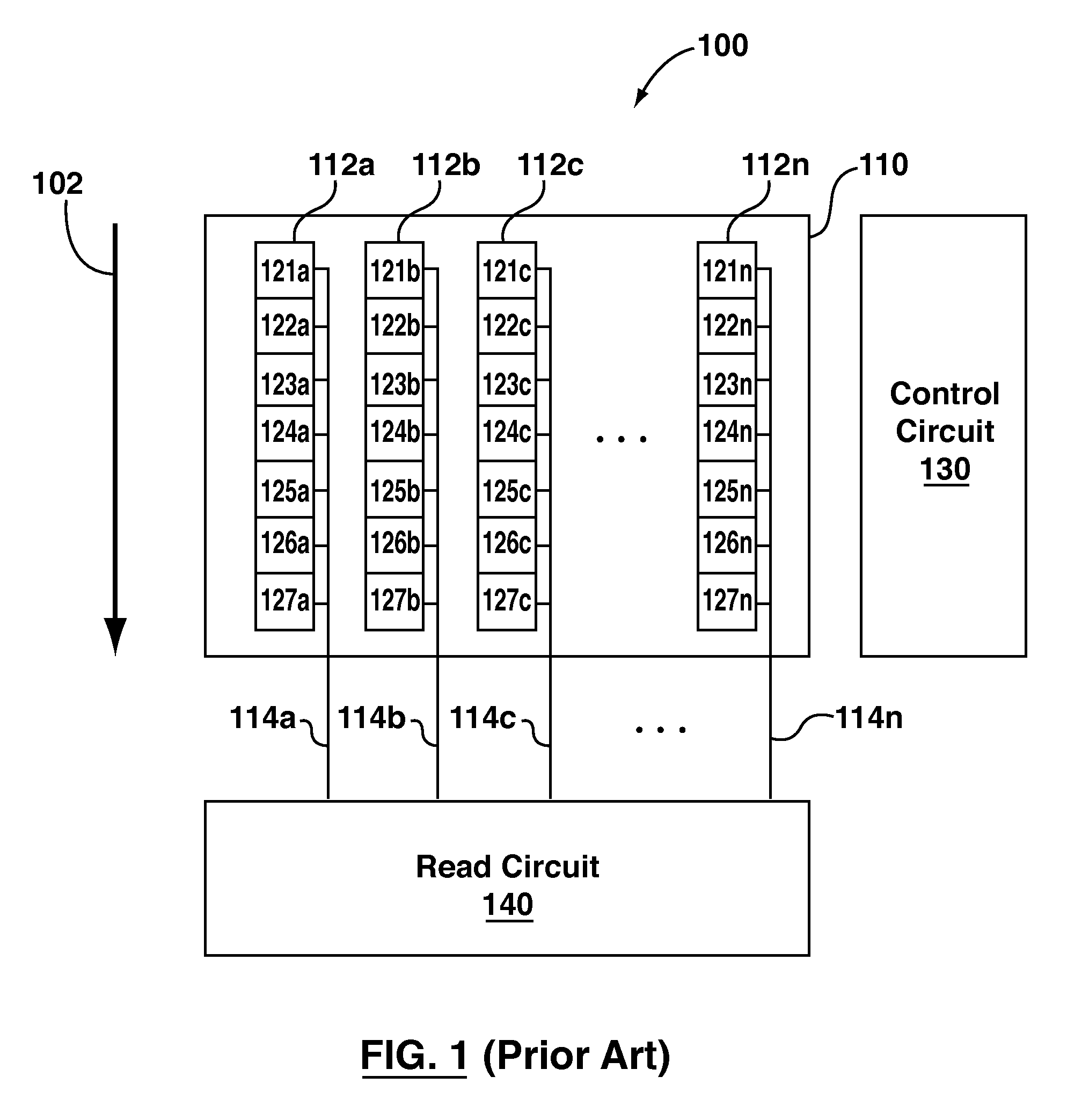
[0018]It will be appreciated that for simplicity and clarity of illustration, where considered appropriate, numerous specific details are set forth in order to provide a thorough understanding of the exemplary embodiments described herein. However, it will be understood by those of ordinary skill in the art that the embodiments described herein may be practiced without these specific details. In other instances, well-known methods, procedures and components have not been described in detail so as not to obscure the embodiments described herein. Furthermore, this description is not to be considered as limiting the scope of the embodiments described herein in any way, but rather as merely describing the implementations of various embodiments described herein.

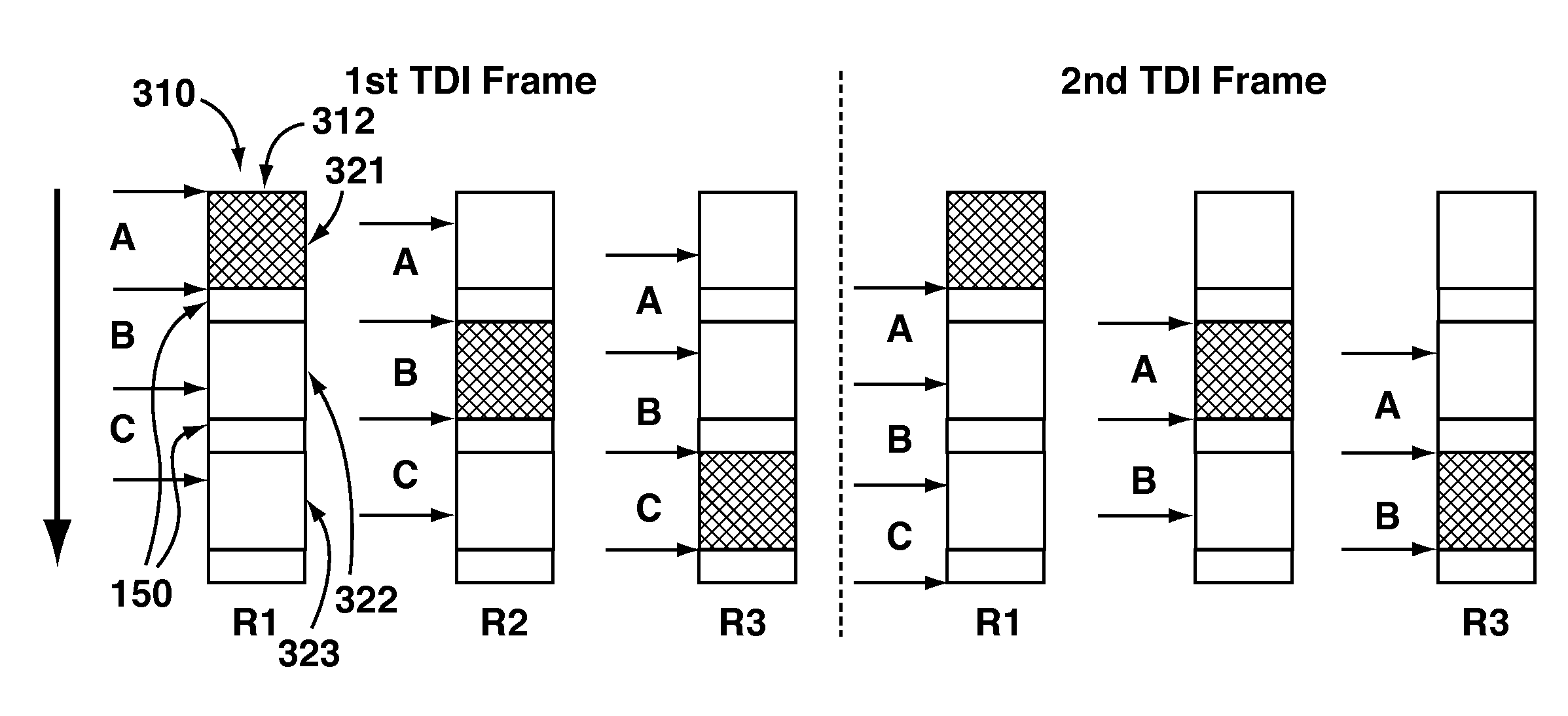
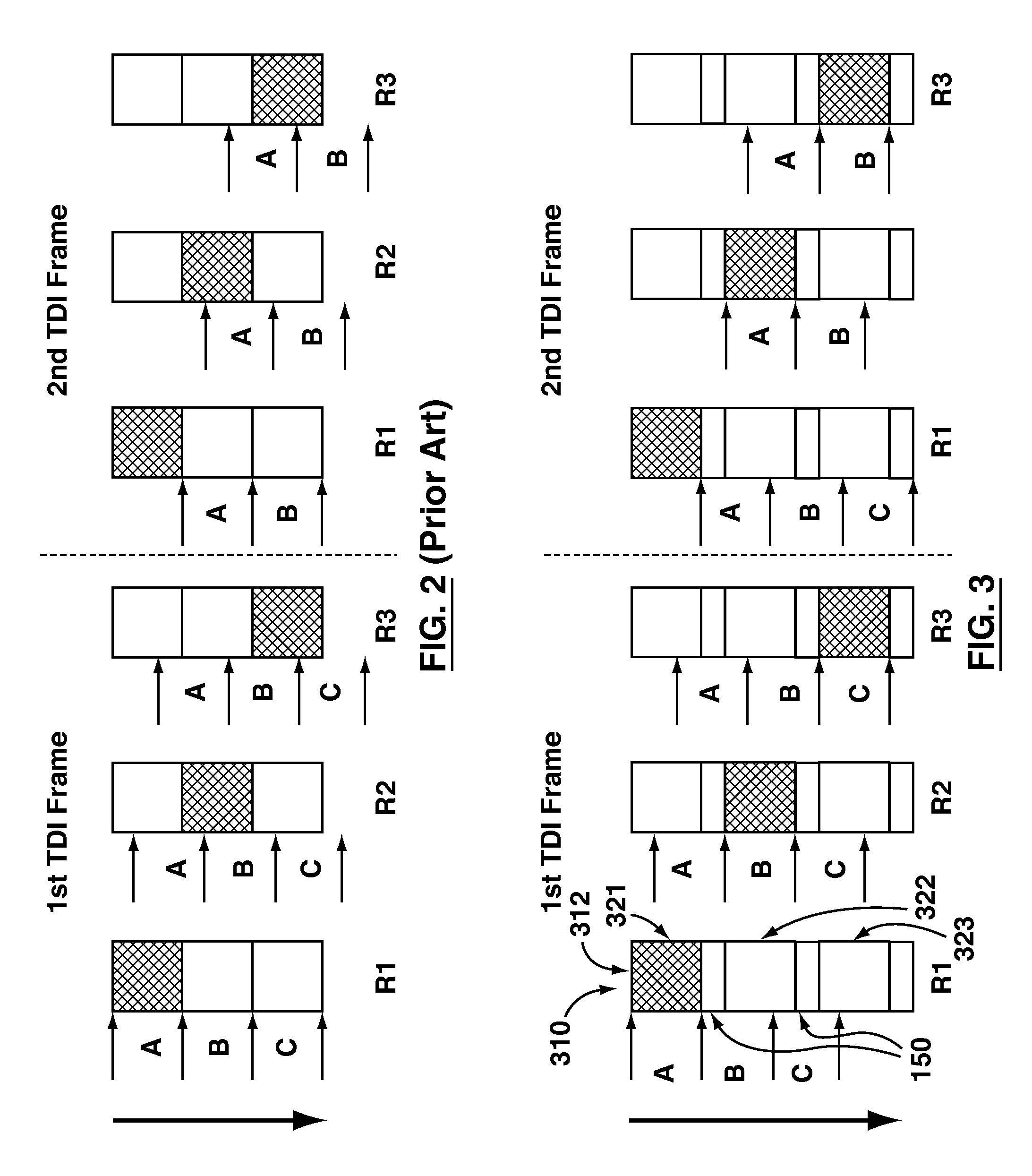
[0019]The term “integration”, as used herein, refers to both charge generation within a CMOS pixel during a period when the pixel is generating photocharge and also to the summing of TDI frames from the photo array. It should be c...


PUM


Abstract

An improved complementary metal oxide semiconductor image sensor for time delay and integration imaging is provided that utilizes rolling shutter pixels. Columns of rolling shutter pixels in the CMOS image array are provided with a space between adjacent pixels to provide synchronization with movement of the subject in the along track direction. Preferably, the physical offset between the pixels is 1 / Nth of a pixel pitch for a column having N rows.

Description

FIELD[0001]The present disclosure relates generally to CMOS image sensors. More particularly, the disclosure relates to CMOS image sensors that implement time delay and integration with rolling shutter pixels.BACKGROUND[0002]Time delay and integration (TDI) is an imaging technique that uses a two-dimensional array image sensor to capture images from an imaging platform that is moving relative to the imaged object or scene. As the object or scene moves across the array, the image sensor takes multiple samples and sums these samples in order to improve the signal to noise ratio as compared to a single frame capture of the image sensor. This improvement to signal to noise ratio makes TDI imaging techniques particularly well-suited to applications with low light levels or fast moving objects. Example applications can include medical imaging, machine vision, roll or conveyor belt inspection systems, or terrestrial imaging from aircraft or satellites.[0003]Conventionally, charge-coupled d...

Claims


Application Information

Patent Timeline
IPC IPC(8): H04N5/376H04N5/374H04N5/378
CPCH04N5/3765H04N5/378H04N5/3743H04N25/768H04N25/78H04N25/745H04N25/75
Inventor FOX, ERIC
Owner TELEDYNE DIGITAL IMAGING INC
Why Eureka
Try Eureka