Polymer/inorganic multi-layer encapsulation film

a multi-layer encapsulation and polymer technology, applied in the direction of transportation and packaging, solid-state devices, semiconductor devices, etc., can solve the problems of difficult use of oled flexible displays, many kinds of polymer substrates, oxygen permeability, etc., to achieve flexibility in the overall layer, suppress oxygen or moisture effectively, and prevent device degradation

Active Publication Date: 2015-11-24
RES & BUSINESS FOUND SUNGKYUNKWAN UNIV
View PDF26 Cites 4 Cited by
  • Summary
  • Abstract
  • Description
  • Claims
  • Application Information

AI Technical Summary

Benefits of technology

[0053]According to the present invention, a multi-layer encapsulation film is provided, which includes a plasma polymer thin film layer formed using a cross-shaped precursor having Si—O bonding, and an inorganic thin film layer, thereby effectively suppressing permeation of oxygen or moisture into an organic electronic device to thus prevent degradation of the device. In the multi-layer encapsulation film according to the present invention, because the plasma polymer thin film layer is very flexible, it achieves flexibility in the overall layer and is therefore suitable for being applied to an organic electronic device. Therefore, it is applicable to various substrates for use in flexible organic electronic devices in display industrial fields. Also in the encapsulation film, the plasma polymer thin film layer is positioned between inorganic thin film layers, thereby remarkably improving encapsulation properties and enhancing durability of bending.

Problems solved by technology

However, organic electronic devices are vulnerable to the permeation of moisture or oxygen.
In particular, many kinds of polymer substrates, due to their high moisture and oxygen permeability, are difficult for use in OLED flexible displays.
Furthermore, because the encapsulation layer is inflexible, it is difficult to apply to flexible devices.
However, this technique is problematic because pinholes may be formed upon deposition of the inorganic thin film, and defects may be caused due to physical damage when applied to flexible devices, undesirably resulting in permeation of moisture and oxygen.
Briefly, functionality of the encapsulation film is easily lost.
However, this method is difficult to apply to production processes because of a low deposition rate of about 0.1 nm per cycle.

Method used


Image

  • Polymer/inorganic multi-layer encapsulation film
  • Polymer/inorganic multi-layer encapsulation film
  • Polymer/inorganic multi-layer encapsulation film

Examples


example 1

Formation of Inorganic Thin Film Layer using Atomic Layer Deposition

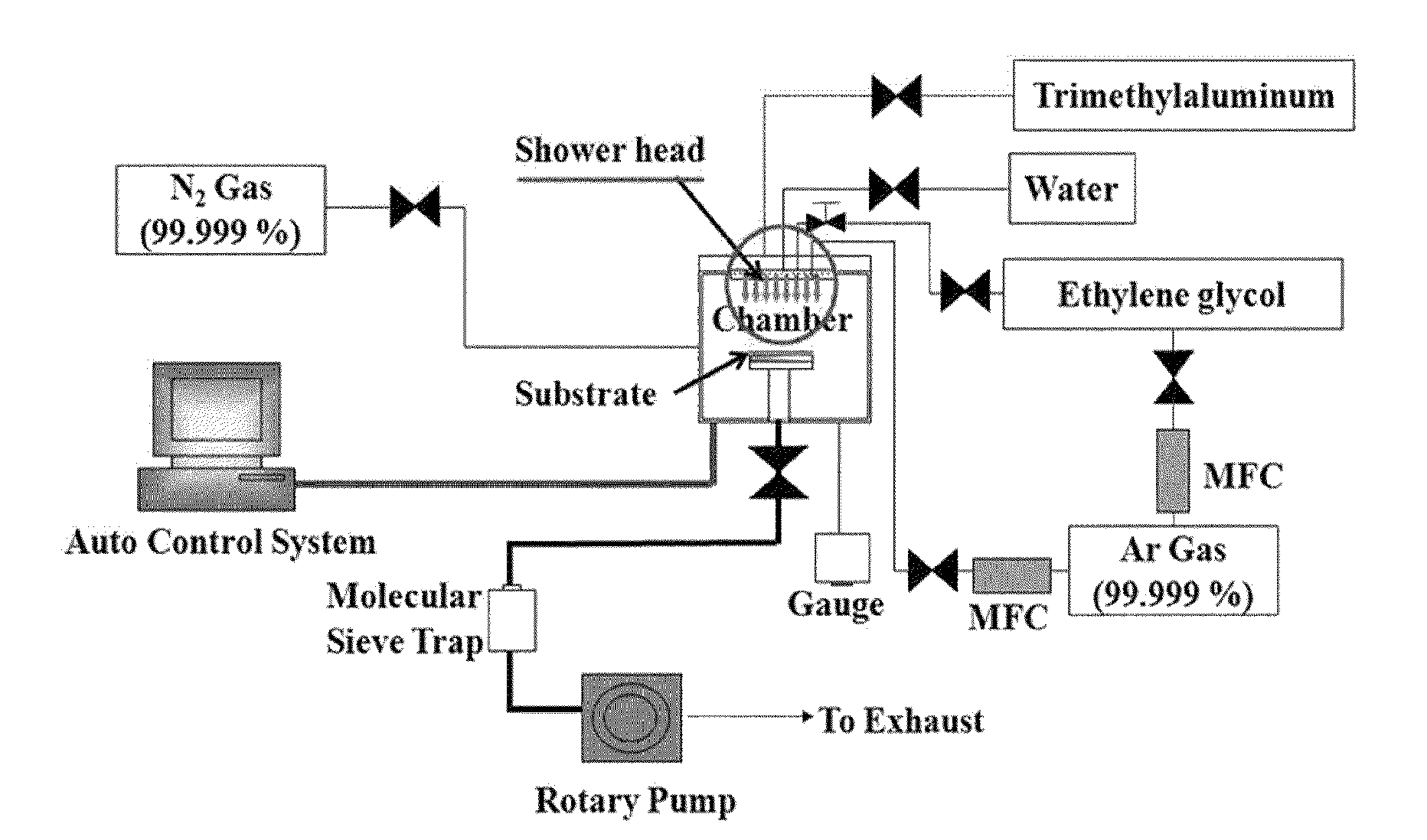
[0064]An inorganic thin film layer was formed by performing atomic layer deposition using an apparatus illustrated in FIG. 1. As such, a vacuum chamber was maintained at 500 mTorr, and trimethyl aluminum and H2O were injected via a difference in pressure from the chamber, thus forming an Al2O3 inorganic thin film. In order to accomplish uniform deposition on the entire surface of polyethylene naphthalate (PEN) used as a plastic substrate, the temperature of the substrate was maintained at 85° C., and thus thermal energy suitable for a chemical reaction was supplied. Furthermore, the injection time of the inorganic material and the purging time of the remaining gas were adjusted, whereby the process conditions (TMA 1 sec—purge 15 sec—H2O 1 sec—purge 15 sec; 1 cycle) were determined. Through one cycle process, a thin film having a thickness of 0.12 nm was deposited, and 200 processes were repeated, thus manufacturing ...

example 2

Formation of Plasma polymer Thin Film Layer using PECVD

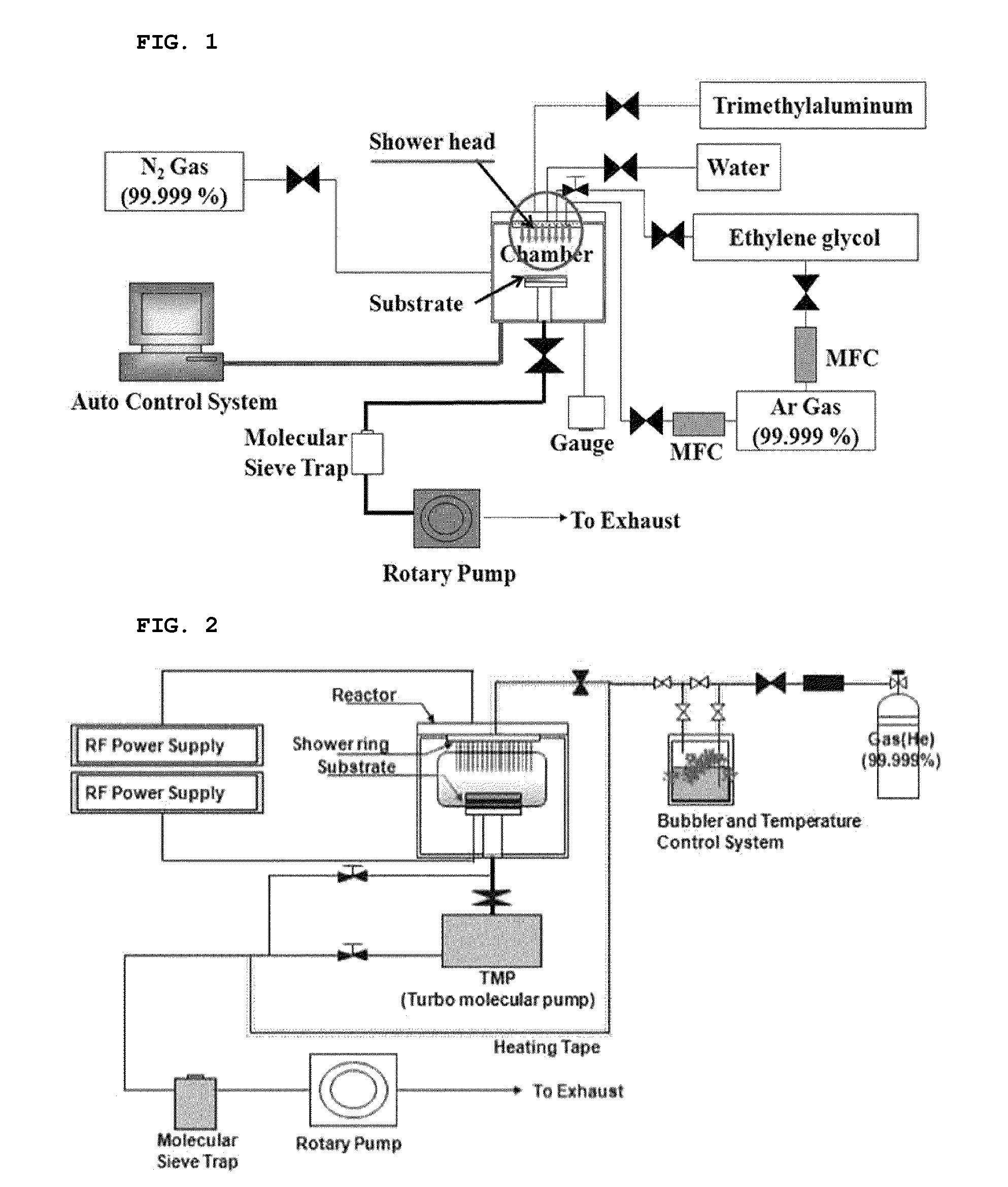
[0065]A plasma polymer thin film layer was formed using a PECVD (Plasma Enhanced Chemical Vapor Deposition) apparatus illustrated in FIG. 2. A plasma polymer thin film deposition process was implemented by means of a process chamber having a chamber lid at the top thereof and a chamber body at the bottom thereof. Used as the precursor of the plasma polymer thin film was tetrakis(trimethylsilyloxy)silane (TTMSS). This precursor was used as a reactive gas, and the reactive gas was uniformly sprayed onto a substrate placed on a substrate susceptor in the chamber body by means of a shower ring provided at the chamber lid maintained at 200 mTorr, thus depositing a thin film. The temperature of 88° C. or higher was maintained so that TTMSS used as the reactive gas was emitted in a vapor state from a bubbler, and the temperature of the line was maintained at 99° C. in order to keep the vapor state even in the line connected up to the c...

example 3

Measurement of Moisture and Oxygen Permeability of Multi-layer Encapsulation Film According to the Present Invention

[0066]The multi-layer encapsulation film manufactured by the method of forming the inorganic thin film layer in Example 1 and the method of forming the plasma polymer thin film layer in Example 2 was measured for moisture and oxygen permeability using Ca-test.

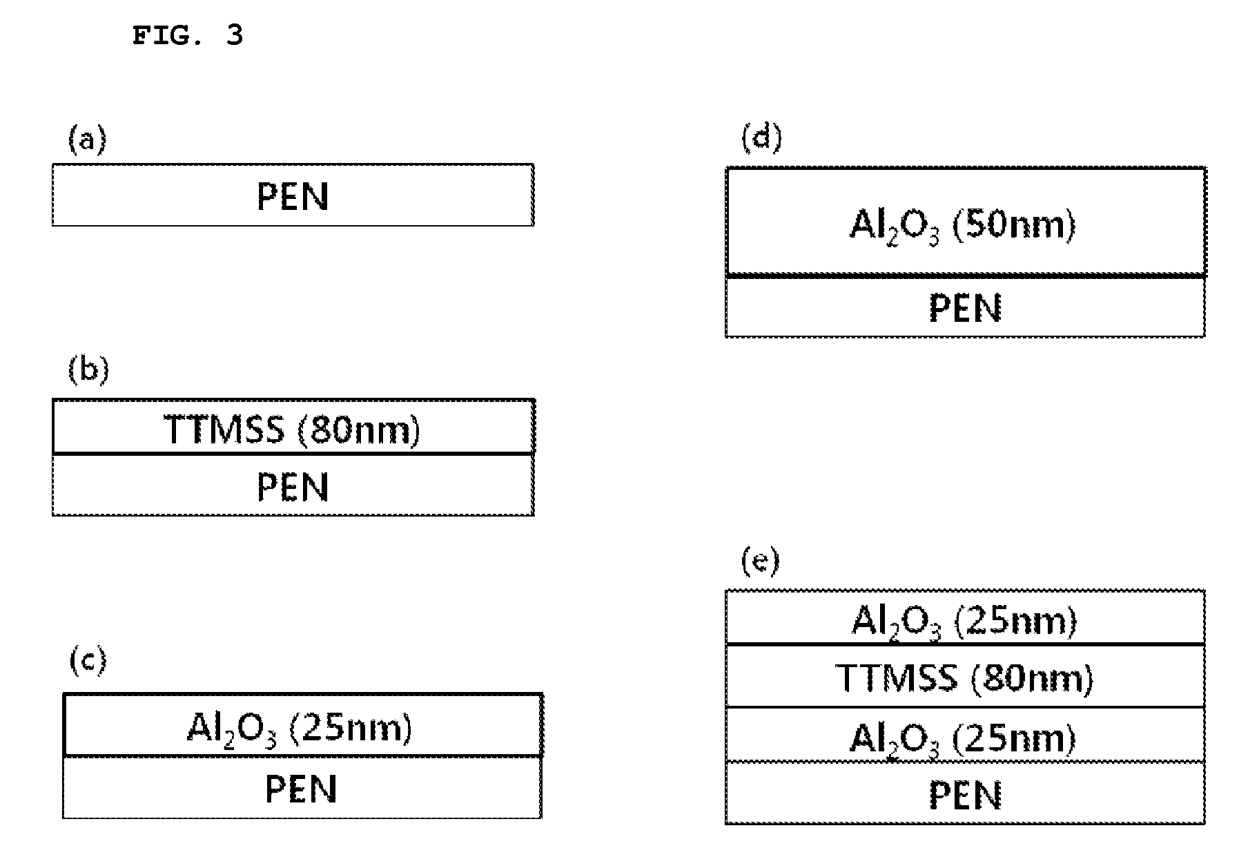
[0067]A variety of films are shown in FIG. 3. FIG. 3(b) illustrates a PEN substrate having a 80 nm thick TTMSS polymer layer deposited thereon, FIG. 3(c) illustrates a PEN substrate having a 25 nm thick Al2O3 layer deposited thereon, FIG. 3(d) illustrates a PEN substrate having a 50 nm thick Al2O3 layer deposited thereon, and FIG. 3(e) illustrates a PEN substrate having a 25 nm thick Al2O3 layer / a 80 nm thick TTMSS polymer layer / a 25 nm Al2O3 layer deposited thereon. The encapsulation properties of these substrates were compared and analyzed using Ca-test equipment illustrated in FIG. 4.

[0068]150 nm thick Al was d...


PUM

PropertyMeasurementUnit
thicknessaaaaaaaaaa
thicknessaaaaaaaaaa
poweraaaaaaaaaa

Abstract

This invention relates to a polymer / inorganic multi-layer encapsulation film, and more particularly, to a multi-layer encapsulation film, which includes a plasma polymer thin film layer formed using a cross-shaped precursor having Si—O bonding and an inorganic thin film layer, and ensures flexibility and has improved encapsulation.

Description

CROSS-REFERENCE TO RELATED APPLICATIONS[0001]This application claims the benefit of Korean Patent Application No. 10-2013-0002648, filed on Jan. 9, 2013 and Korean Patent Application No. 10-2013-0122884, filed on Oct. 15, 2013, in the Korean Intellectual Property Office, the entire disclosures of which are incorporated herein by reference for all purposes.TECHNICAL FIELD[0002]The present invention relates to a polymer / inorganic multi-layer encapsulation film, which ensures flexibility and has improved encapsulation properties.BACKGROUND ART[0003]Techniques of producing organic electronic devices using organic materials enable the integration of displays, circuits, cells, sensors, etc. on flexible plastic substrates at low temperatures, approximately equivalent to room temperature, by the use of coating and printing processes. These techniques are advantageous because electronic devices may be inexpensively formed on large flexible substrates.[0004]However, organic electronic devices...

Claims


Application Information

Patent Timeline
Patent Type & Authority Patents(United States)
IPC IPC(8): H01L51/10H01L51/44H01L51/52
CPCH01L51/107H01L51/448H01L51/5253Y02E10/549Y10T428/269Y10T428/31507Y10T428/31663H10K10/88H10K77/111H10K30/88H10K50/8445H10K2102/311H10K50/844
Inventor JUNG, DONG GEUNCHAE, HEEYEOPPARK, MIN WOOKIM, HOON BAELEE, CHAE MIN
Owner RES & BUSINESS FOUND SUNGKYUNKWAN UNIV
Why Eureka
Try Eureka