
Nano-capacitor arrays for energy storage using native aluminum oxide layers and other ultra-thin dielectrics

a technology of aluminum oxide and dielectric arrays, which is applied in the direction of fixed capacitor dielectrics, fixed capacitor details, multi-fixed capacitors, etc., can solve the problems of increasing the gap size between electrodes separated by solid dielectrics, and unable to address the enhancement of dielectric strength with decreasing the gap size between electrodes, so as to reduce localized heating energy and enhance energy storage

Inactive Publication Date: 2015-12-22
THE BOARD OF TRUSTEES OF THE UNIV OF ILLINOIS
View PDF2 Cites 2 Cited by
  • Summary
  • Abstract
  • Description
  • Claims
  • Application Information

AI Technical Summary

Benefits of technology

This patent talks about ways to improve the performance of a device called nanocapacitors. First, it mentions that the device can have fuses on each nanocapacitor cell or groups of cells to help it operate at a higher voltage by eliminating defective cells. This would reduce the risk of the device being unable to operate properly due to faulty cells. The fuses can be made of different materials like tellurium, polysilicon, silicon, or metals like aluminum or copper. Additionally, the patent suggests placing the device in a colder environment (like liquid nitrogen or liquid oxygen) and cooling it using convection particles to reduce heating and prevent damage to the nanocapacitors. These improvements would make the device more reliable and efficient.

Problems solved by technology

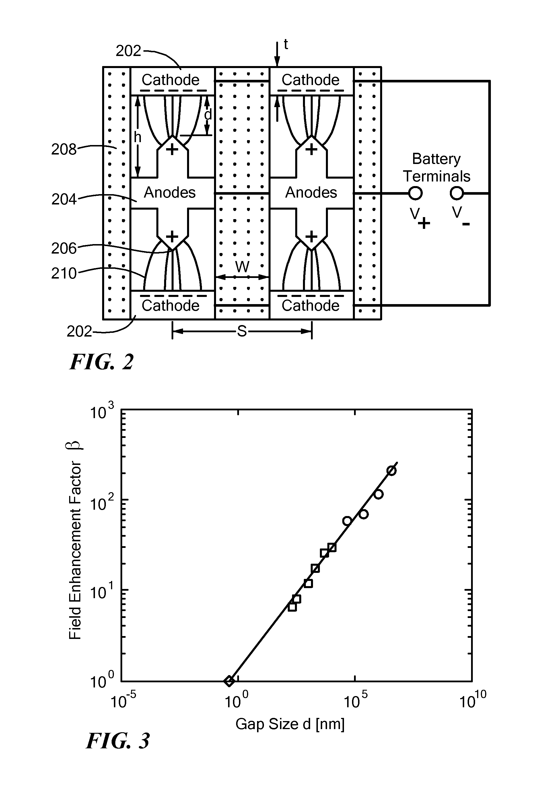
42-46 (2007), nanomaterials have been used to increase charge density, however the enhancement of dielectric strength with decreasing gap size between electrodes separated by a solid dielectric has never been addressed.

Method used


Image

  • Nano-capacitor arrays for energy storage using native aluminum oxide layers and other ultra-thin dielectrics
  • Nano-capacitor arrays for energy storage using native aluminum oxide layers and other ultra-thin dielectrics
  • Nano-capacitor arrays for energy storage using native aluminum oxide layers and other ultra-thin dielectrics

Examples


Embodiment Construction

[0006]The present invention relates to nano capacitors with solid or partial-vacuum dielectrics.

[0007]As used herein and in any appended further description or claims, the term “nano-capacitor” is used interchangeably with the term “nanocapacitor.” The meaning of the term is that of a capacitor characterized by at least one dimension in the range between 0.1 nanometers and 1000 nanometers.

[0008]As used herein and in any appended claims, the term “electron mean free path” (MFP), used interchangeably with “electron inelastic mean free path” (IMFP), as applied to electrons traveling in a specified dielectric of any phase of matter, shall refer to the distance an electron may travel in the dielectric before the probability of its losing energy to scatter reaches 1 / e, where e is Euler's constant. The probability of scatter is 1−e−d / λ(E), where λ(E) is the MFP of an electron at incident energy E. The electron loses energy due to such processes as electron-hole formation in the dielectric ...


PUM

PropertyMeasurementUnit
Thicknessaaaaaaaaaa
Thicknessaaaaaaaaaa
Dielectric strengthaaaaaaaaaa

Abstract

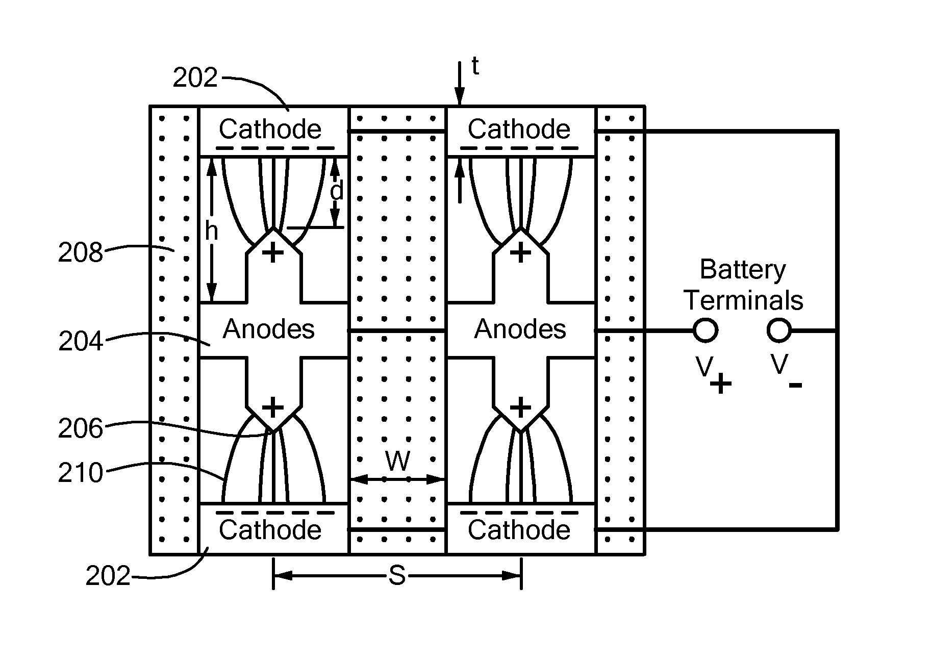
Methods and apparatus for storing information or energy. An array of nano-capacitors is provided, where each nano-capacitor has a cathodic electrode and an anode separated by a dielectric. The thickness of the intervening solid dielectric is in the range between 0.1 nanometers and 1000 nanometers and is shorter than an electron mean free path within the dielectric. The cathodic electrode is at least 100 times larger than the thickness of the intervening dielectric in every direction transverse to the thickness of the intervening dielectric. An excess of electrons is stored on the cathodic electrode. The dielectric may be a metal oxide, particularly a native oxide of the cathode material.

Description

[0001]The present Application is a continuation-in-part application of U.S. Ser. No. 12 / 908,107, now issued as U.S. Pat. No. 8,699,206, and, through that application, claims priority from U.S. Provisional Patent Application Ser. No. 61 / 253,605, filed Oct. 21, 2009. Additionally, the present Application claims the priority of U.S. Provisional Patent Application Ser. No. 61 / 774,133, filed Mar. 7, 2013. All of the foregoing applications are incorporated herein by reference.TECHNICAL FIELD[0002]The present invention relates to devices and methods for high-density storage of energy in materials configured as nano-capacitors subject to specified material and geometrical properties.[0003]This invention was made with government support under Grant DMS 03-25939 ITR, awarded by the National Science Foundation and under Contract No. 1-485927-244014-191100, awarded by the U.S. Air Force. The Government has certain rights in the invention.BACKGROUND ART[0004]In supercapacitors and ultracapacitor...

Claims


Application Information

Patent Timeline
IPC IPC(8): H01G4/06H01G4/38H01G4/10H01G4/12
CPCH01G4/06H01G4/38H01G4/12H01G4/10
Inventor HUBLER, ALFRED W.
Owner THE BOARD OF TRUSTEES OF THE UNIV OF ILLINOIS
Learn More