Thin film photovoltaic cell structure, nanoantenna, and method for manufacturing

a thin film photovoltaic cell and nanoantenna technology, applied in the field of thin film photovoltaic cells, can solve the problems of different surface textures, inconvenient use of thin film configurations, and inability to meet the requirements of manufacturing tolerances of single antenna units, so as to facilitate cost-efficient industrial-scale manufacturing and improve light capture efficiency.

Inactive Publication Date: 2016-02-02
AALTO UNIV FOUND
View PDF8 Cites 0 Cited by
  • Summary
  • Abstract
  • Description
  • Claims
  • Application Information

AI Technical Summary

Benefits of technology

[0014]The object of the present invention is to provide a thin film photovoltaic cell structure with improved light capturing efficiency and enabling cost-efficient industrial-scale manufacturing. Another object of the present invention is to provide a nanoantenna which is suitable, for example, for use in such thin film photovoltaic cell structures. It is also an object of the present invention to provide a cost-efficient method for manufacturing such thin film photovoltaic cells.SUMMARY OF THE INVENTION

Problems solved by technology

This is an important issue in all photovoltaic cell configurations.
On the other hand, light capturing solutions used with conventional thick film cells, e.g. different surface textures for coupling the incident light into the cell, are usually not suitable for thin film configurations.
Moreover, single antenna units are not very sensitive to the manufacturing tolerances thereof.
On the other hand, also the known nanoantenna configurations suffer from a narrow wavelength / frequency band of the plasmon resonance.
However, they comprise complex multilayer structures located on both sides of the active photovoltaic region, the multilayer structures necessitating nanometer-scale precision of manufacture.
The costs of such cavities are comparable with the costs of the regular plasmonic light concentrators, thus making them unsuitable for use in typically very cost-critical thin-film solar cells.

Method used


Image

  • Thin film photovoltaic cell structure, nanoantenna, and method for manufacturing
  • Thin film photovoltaic cell structure, nanoantenna, and method for manufacturing
  • Thin film photovoltaic cell structure, nanoantenna, and method for manufacturing

Examples


Embodiment Construction

[0048]Preferred embodiments of the present invention are described in more detail in the following with reference to the accompanying figures, wherein

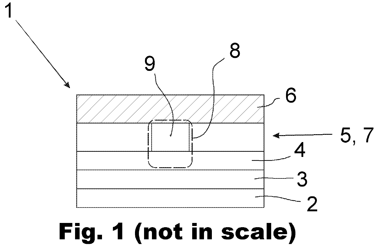
[0049]FIG. 1 illustrates a thin film photovoltaic cell structure according to the present invention;

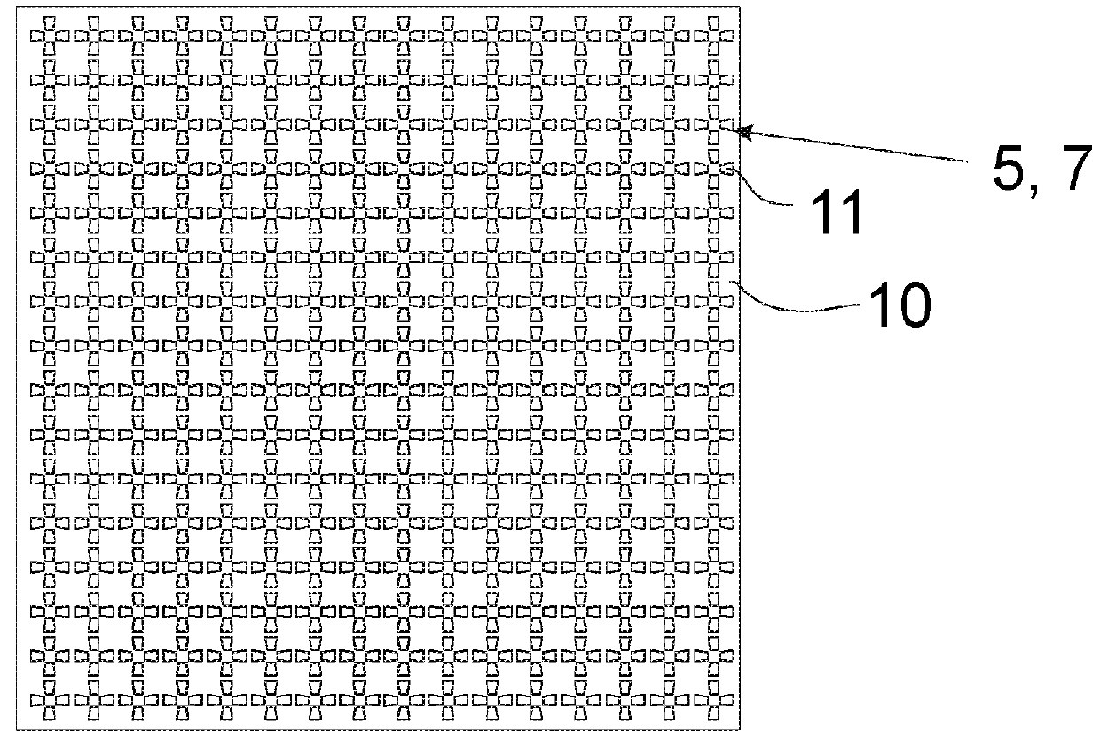
[0050]FIG. 2 shows a plasmonic light concentrator arrangement of the thin film photovoltaic cell structure of FIG. 1;

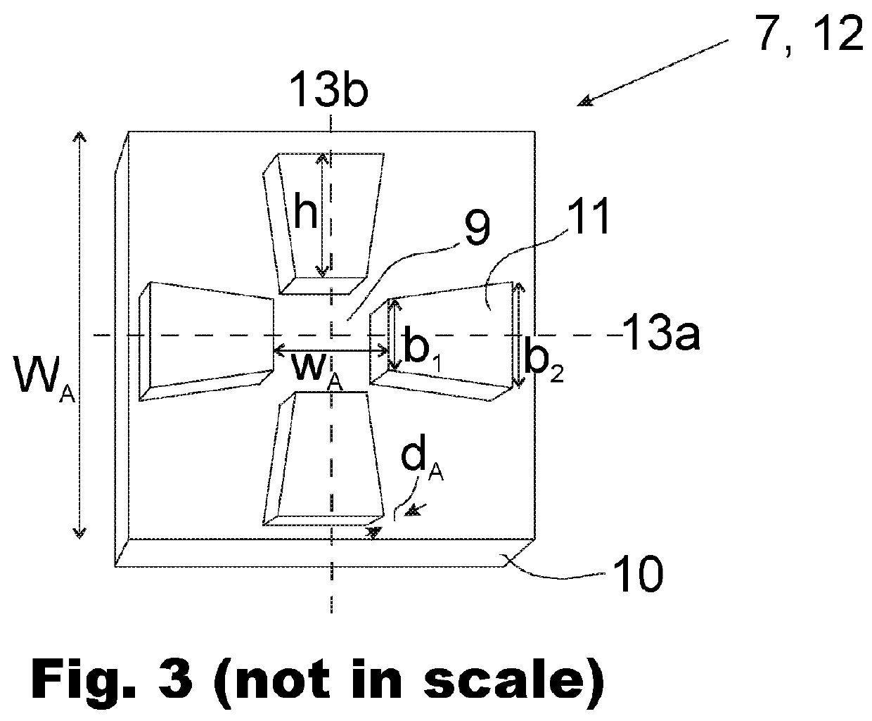
[0051]FIG. 3 shows a nanoantenna forming a part of the plasmonic light concentrator arrangement of FIG. 2;

[0052]FIG. 4 represents simulation results of a nanoantenna according to FIG. 3;

[0053]FIG. 5 shows a modified version of the nanoantenna geometry of FIG. 3;

[0054]FIG. 6 shows another nanoantenna suitable for a plasmonic light concentrator arrangement according to the present invention;

[0055]FIG. 7 illustrates manufacturing of a thin film photovoltaic cell structure according to the present invention;

[0056]FIGS. 8 and 9 illustrate, as schematic drawings, examples of implementing a thin film photovoltaic cell comprising ...


PUM


Abstract

A thin film photovoltaic cell structure (1) comprises a substrate (2); a first dielectric layer (3) on the substrate (2); an active layer (4) on the first dielectric layer (3); and a plasmonic light concentrator arrangement (5) on the active layer (4) for coupling incident light at a first wavelength band into the active layer (4). According to the present invention, the thin film photovoltaic cell structure (1) further comprises a second dielectric layer (6) formed of a dielectric material which is transparent at the first wavelength band and at a second wavelength band on the plasmonic light concentrator arrangement (5); the first dielectric layer (3), the active layer (4), the plasmonic light concentrator arrangement (5), and the second dielectric layer (6) being configured to form a resonant cavity for coupling incident light at the second wavelength band into a standing wave confined in the resonant cavity.

Description

FIELD OF THE INVENTION[0001]The present invention relates to thin film photovoltaic cells, particularly to plasmon-enhanced thin film photovoltaic cells. The present invention also relates to nanoantennas for plasmonic light concentrator arrangements for thin film photovoltaic cells. The present invention further relates to manufacturing of plasmon-enhanced photovoltaic cells.BACKGROUND OF THE INVENTION[0002]Photovoltaic cells are used in a great variety of applications to convert electromagnetic radiation, e.g. the solar radiation, to electrical energy.[0003]By a photovoltaic cell is meant here generally a semiconductor-based component converting incident electromagnetic radiation to electrical energy through a photovoltaic effect. In the case of solar radiation as the primary energy source, a photovoltaic cell is usually called a solar cell. In general, a photovoltaic cell comprises a p-type semiconductor region, an n-type semiconductor region, and an active region. The n-type and...

Claims


Application Information

Patent Timeline
Patent Type & Authority Patents(United States)
IPC IPC(8): B82Y20/00G02B5/00H01L31/0232H01L31/0392H01L31/054
CPCH01L31/02327B82Y20/00G02B5/008H01L31/0392H01L31/0543Y02E10/52
Inventor SIMOVSKI, CONSTANTIN
Owner AALTO UNIV FOUND
Why Eureka
Try Eureka