A1-doped ZNO transparent conductive micro/nano wire array film and preparation method thereof

A nanowire array, transparent and conductive technology, applied in semiconductor/solid-state device manufacturing, nanotechnology, circuits, etc., can solve the problems of low deposition rate, non-existence, and good crystallinity of TCO thin films

Active Publication Date: 2016-05-04
CHANGSHA UNIVERSITY OF SCIENCE AND TECHNOLOGY
View PDF4 Cites 0 Cited by
  • Summary
  • Abstract
  • Description
  • Claims
  • Application Information

AI Technical Summary

Problems solved by technology

The TCO film prepared by magnetron sputtering, electron beam evaporation, PLD and MOCVD has good crystallinity and low resistivity. Among them, magnetron sputtering is the most mature process at present, but all of them have large investment, complicated equipment, Disadvantages such as low deposition rate and small deposition area
The sol-gel method and spray pyrolysis method can realize large-area film formation and low-cost preparation of TCO thin films, but the quality of film formation is poor, and the resistivity of the prepared film is high
Electrodeposition can be used to form dense ZnO thin films or ZnO nanowire array films at low cost and large area, but there is no literature report on the growth of doped ZnO micro / nanowire (or rod) array films by electrodeposition.

Method used


Image

  • A1-doped ZNO transparent conductive micro/nano wire array film and preparation method thereof
  • A1-doped ZNO transparent conductive micro/nano wire array film and preparation method thereof
  • A1-doped ZNO transparent conductive micro/nano wire array film and preparation method thereof

Examples


Embodiment 1

[0053] A growth process condition and steps of an undoped ZnO thin film of the present invention:

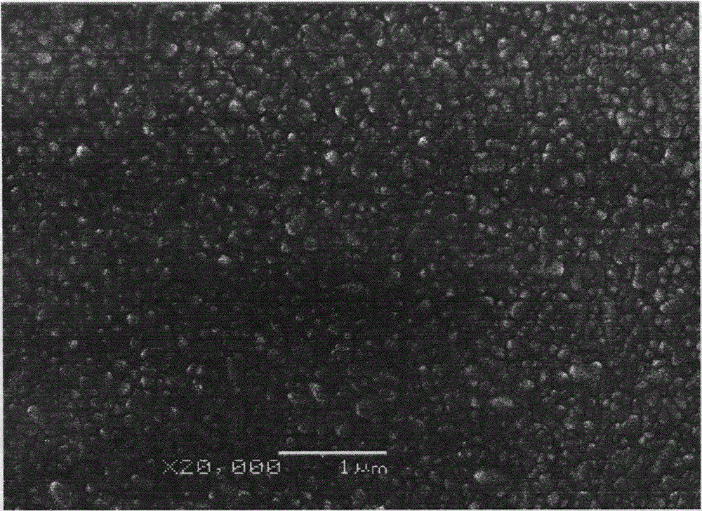
[0054] (1) Substrate: Fluorine-doped tin oxide (SnO 2 : F, FTO) glass, the sheet resistance is 18Ω / □, the surface morphology is as figure 2 shown;

[0055] (2) Solution system: Zn(NO 3 ) 2 Aqueous solution, concentration 0.025M;

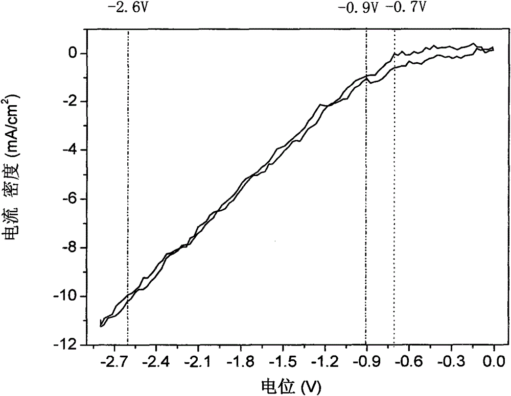
[0056] (3) Electrodeposition process conditions: the distance between the plates is 3cm, the cathode potential is -2.5V, the electrodeposition temperature is 80±3°C, and the electrodeposition time is 20min;

[0057] (4) Crystallization heat treatment conditions: 530°C, heat preservation for 1h, air atmosphere, cooling with the furnace;

[0058] (5) Heat treatment under vacuum conditions: 450°C, heat preservation for 0.5h, vacuum, cooling down with the furnace.

[0059] The morphology of the prepared ZnO nanorod array film sample is as follows: image 3 As shown, the sheet resistance is 20kΩ / □, and the visible light transmittance is less than 60...

Embodiment 2

[0061] A growth process condition and steps of a transparent conductive Al-doped ZnO nanowire array film of the present invention:

[0062] (1) FTO glass substrate (with example 1);

[0063] (2) Solution system: Zn(NO 3 ) 2 with Al(NO 3 ) 3 Mixed aqueous solution, concentration 0.003M, Al / Zn atomic ratio = 3.3%;

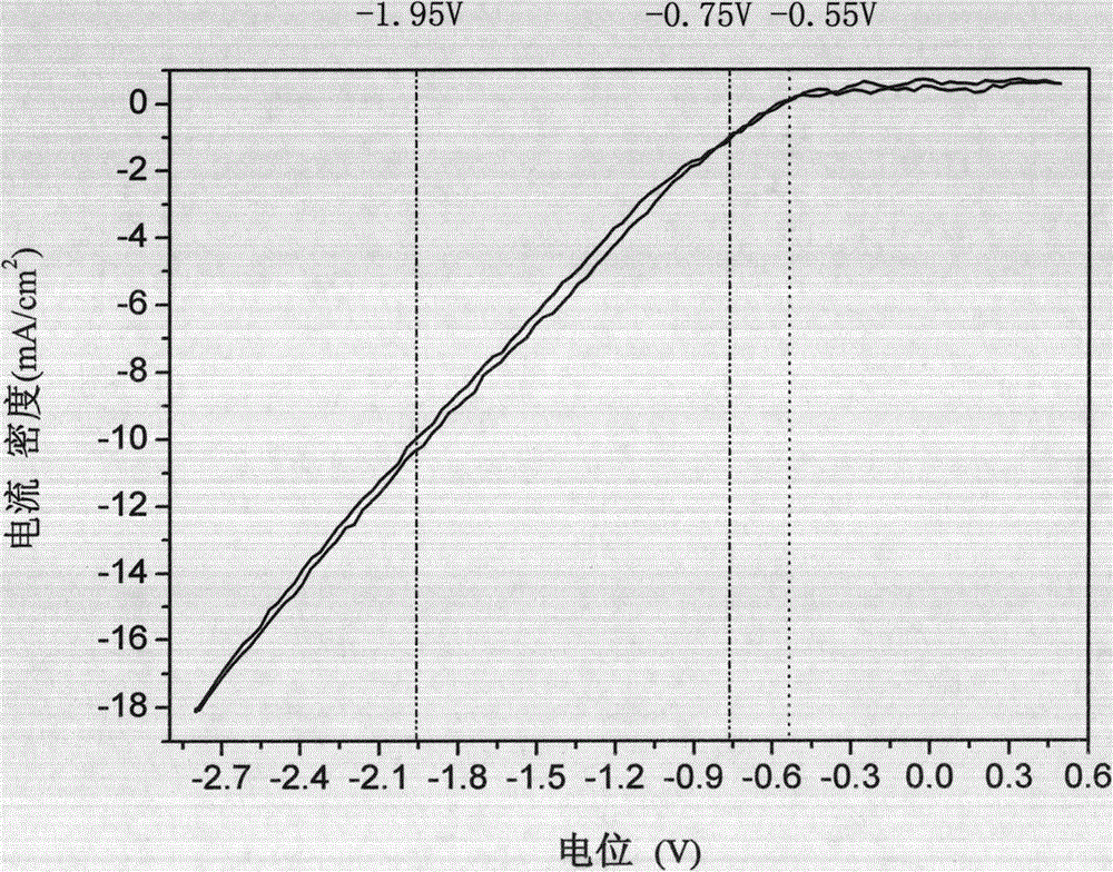
[0064] (3) Electrodeposition process conditions: the distance between the plates is 2cm, the cathode potential is -1.5V, the electrodeposition temperature is 80±3°C, and the electrodeposition time is 1h;

[0065] (4) Crystallization heat treatment conditions: 530°C, heat preservation for 1h, air atmosphere, cooling with the furnace;

[0066] (5) Heat treatment under vacuum conditions: 450°C, heat preservation for 0.5h, vacuum, cooling down with the furnace.

[0067] The prepared ZnO: Al nanowire array film sample morphology is as follows Figure 4 As shown, the sheet resistance is 180Ω / □ (compared with the undoped ZnO thin film, the sheet resistance is reduced...


PUM


Abstract

The invention provides an Al doped ZnO transparent conducting micrometer / nanometer wire array film and a preparation method thereof. The array film has excellent conductivity and visible light transparency and has the texture light trapping effect of a micrometer / nanometer wire array film at the same time.

Description

technical field [0001] The invention relates to the field of new energy materials, in particular to a transparent conductive oxide thin film with a special appearance and structure applied to thin-film solar cells and a growth method thereof. Background technique [0002] Transparent Conductive Oxide (TCO for short) is a kind of visible light transparent wide bandgap oxide semiconductor material with excellent conductivity obtained by doping or other defect chemical principles. TCO thin films have both light transmission and conductivity, and can be widely used as transparent electrodes for optoelectronic devices. The existing TCO thin film material system mainly includes SnO 2 、In 2 o 3 , ZnO, CdO, etc. and their composite oxides wide bandgap oxide semiconductors (E g >3eV), by introducing non-stoichiometric ratio or appropriate doping, they have high visible light transmittance (λ=380nm~780nm, >80%) and low resistivity (<10 -3 Ω·cm) characteristics. [0003]...

Claims


Application Information

Patent Timeline
Patent Type & Authority Patents(China)
IPC IPC(8): H01L31/0224H01L31/0216H01L31/0232H01L31/02H01L31/18H01L21/208B82Y40/00
CPCY02P70/50
Inventor 陈建林陈荐郭辰熹胡琳琳唐植懿
Owner CHANGSHA UNIVERSITY OF SCIENCE AND TECHNOLOGY
Why Eureka
Try Eureka