Polishing method and polishing apparatus

a technology of polishing apparatus and polishing method, which is applied in the direction of lapping machines, grinding machine components, manufacturing tools, etc., can solve the problems of inability to measure the thickness at the same position under the same conditions, and the film thickness measuring device incorporated in the cmp apparatus may fail to measure the thickness, so as to prevent the failure of detection of the polishing end point

Active Publication Date: 2016-02-23
EBARA CORP
View PDF27 Cites 4 Cited by
  • Summary
  • Abstract
  • Description
  • Claims
  • Application Information

AI Technical Summary

Benefits of technology

[0007]It is therefore an object to provide a polishing method and a polishing apparatus capable of obtaining an accurate thickness of a film (e.g., the dielectric film, the metal film, or the silicon layer) formed on the substrate during polishing of the substrate and capable of accurately determining a substrate polishing end point based on the thickness of the film obtained.
[0018]According to the above-described embodiments, the following effects can be obtained.
[0022](4) If the defective data rate has reached the predetermined upper limit during polishing of the substrate, the alarm signal is emitted. Therefore, a detection failure of the polishing end point can be prevented.

Problems solved by technology

However, the film-thickness measuring device incorporated in the CMP apparatus may fail to measure the thickness if there is a variation in the thickness of the film because it measures the thickness of the film while the device itself is moving as shown in FIG. 1.
Moreover, since the film is scraped away every time the polishing table makes one revolution, it is impossible to measure the thickness at the same position under the same conditions.

Method used


Image

  • Polishing method and polishing apparatus
  • Polishing method and polishing apparatus
  • Polishing method and polishing apparatus

Examples


Embodiment Construction

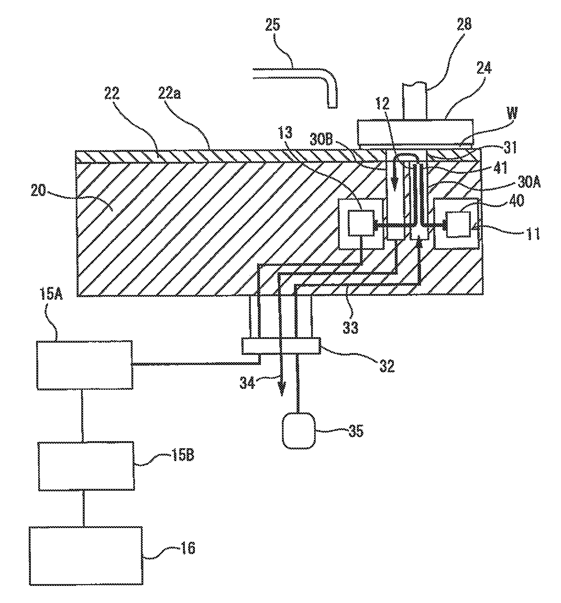
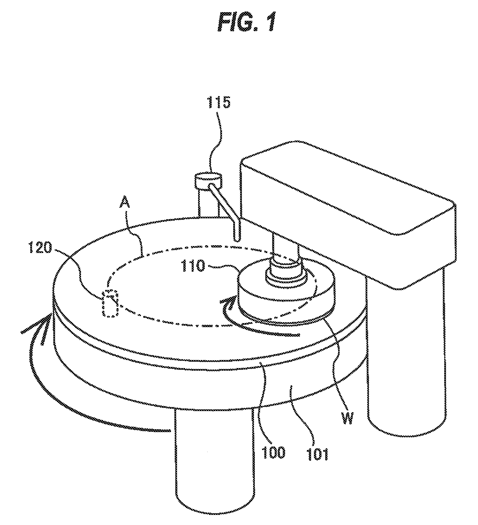
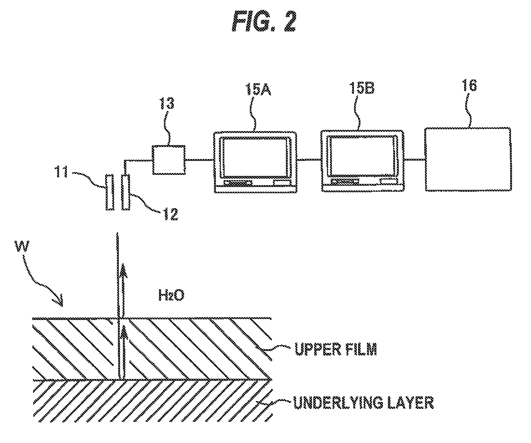
[0046]Embodiments of the present invention will be described below with reference to the drawings. FIG. 2 is a schematic view for illustrating the principle of an optical polishing end point detection method, and FIG. 3 is a plan view showing positional relationship between wafer and polishing table. As shown in FIG. 2, a wafer W has an underlying layer and a film formed on the underlying layer. The wafer W is held by a top ring (not shown in FIGS. 2 and 3) and rotated about its central axis as shown in FIG. 3. A surface of the wafer W is pressed by the top ring against a polishing pad 22 on a rotating polishing table 20, so that the film of the wafer W is polished by sliding contact with the polishing pad 22, which is a polishing tool having a polishing surface for polishing the wafer W. A grindstone (or fixed abrasive) may be used as the polishing tool, instead of the polishing pad 22.

[0047]An irradiator 11 and an optical receiver 12 are disposed in the polishing table 20 and are ...


PUM


Abstract

A method of polishing a substrate is disclosed. The method includes irradiating the substrate with light; measuring intensity of the reflected light; producing spectral waveform representing relationship between relative reflectance and wavelength of the light; performing a Fourier transform process on the spectral waveform to determine a thickness of the film and a corresponding strength of frequency component; determining whether the determined thickness of the film is reliable or not by comparing the strength of frequency component with a threshold value; calculating a defective data rate representing a proportion of the number of unreliable measured values to the total number of measured values; and changing the threshold value based on the defective data rate.

Description

CROSS REFERENCE TO RELATED APPLICATION[0001]This application claims priority to Japanese Patent Application No, 2013-092183 filed Apr. 25, 2013, the entire contents of which are hereby incorporated by reference.BACKGROUND[0002]Semiconductor devices are fabricated through several processes including a process of polishing a dielectric film, e.g., SiO2, and a process of polishing a meta film, e.g., copper or tungsten. Fabrication processes of backside illumination CMOS sensor and through-silicon via (TSV) include a process of polishing a silicon layer (silicon wafer), in addition to the polishing processes of the dielectric film and the metal film.[0003]Polishing of the wafer is terminated when a thickness of a film (e.g., the dielectric film, the metal film, or the silicon layer), constituting a wafer surface, has reached a predetermined target value. CMP (Chemical Mechanical Polishing) apparatus is used for polishing the wafer. FIG. 1 is a schematic view of the CMP apparatus. The CM...

Claims


Application Information

Patent Timeline
Patent Type & Authority Patents(United States)
IPC IPC(8): B24B37/00B24B49/12H01L21/306B24B37/013
CPCB24B37/013B24B49/12H01L21/30625B24B37/005B24B37/042
Inventor KIMBA, TOSHIFUMI
Owner EBARA CORP
Why Eureka
Try Eureka