Quad flat no lead package and production method thereof

a flat-type, lead-free technology, applied in the direction of semiconductor devices, semiconductor/solid-state device details, electrical equipment, etc., can solve the problems of high welding wire cost, limited frequency application, long welding wire, etc., to achieve a smaller volume, light weight, and more i/o number

Active Publication Date: 2016-03-01
TIANSHUI HUATIAN TECH +1
View PDF7 Cites 1 Cited by
  • Summary
  • Abstract
  • Description
  • Claims
  • Application Information

AI Technical Summary

Benefits of technology

[0032]According to the production method of the present invention, laser cutting is adopted to separate the leads so as to realize lead separation and prepare a package having multi-circle arranged lead frames. The package has more I / O number, smaller volume, lighter weight as well as excellent electrical property and thermal property, and is particularly suitable for any application having requirements on size, weight and property. According to the package, the problems of few pins, long bonding wire, high welding cost and limited frequency application during single-face packaging of the existing normal quad flat no lead package (QFN) are solved.

Problems solved by technology

For a long time, a single circle lead frame mode is always continued for QFN products due to the limitation of etching templates and etching process.
However, the present quad flat no lead package has the defects of few leads (namely, few I / O), long welding wire, high welding wire cost, and limited frequency application, which cannot meet the demands of high density and multiple I / O packaging.

Method used


Image

  • Quad flat no lead package and production method thereof
  • Quad flat no lead package and production method thereof
  • Quad flat no lead package and production method thereof

Examples


embodiment 1

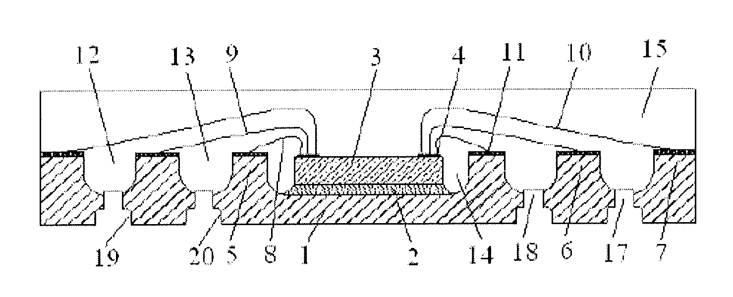
[0097]Adopt an ordinary QFN thinning method to thin a wafer to obtain a wafer having a final thickness of 150 μm˜200 μm, wherein a rough polishing range is from original wafer+adhesive film to final thickness+adhesive film thickness+50 μm, a rough polishing speed is 3 μm / s˜6 μm / s, a rough polishing speed is 3 μm / s, a fine grinding thickness range is from 155 μm+adhesive film thickness to 150 μm+adhesive film thickness, and a fine grinding speed is 10 μm / min. Adopt a breakage-proof process and adopt a DISC 3350 scribing machine to perform scribing on the thinned wafer to obtain an IC chip, wherein a breakage-proof and anti-cracking scribing process software control technique is adopted, and a scribing feeding speed is ≦10 mm / s.

[0098]Manufacture a Lead Frame Carrier.

[0099]First step: take a copper plate having a thickness of 6 mil, and pretreat the surface of the copper plate including degreasing, micro corrosion, pickling and washing, removing oil stain, fingerprints and oxides on th...

embodiment 2

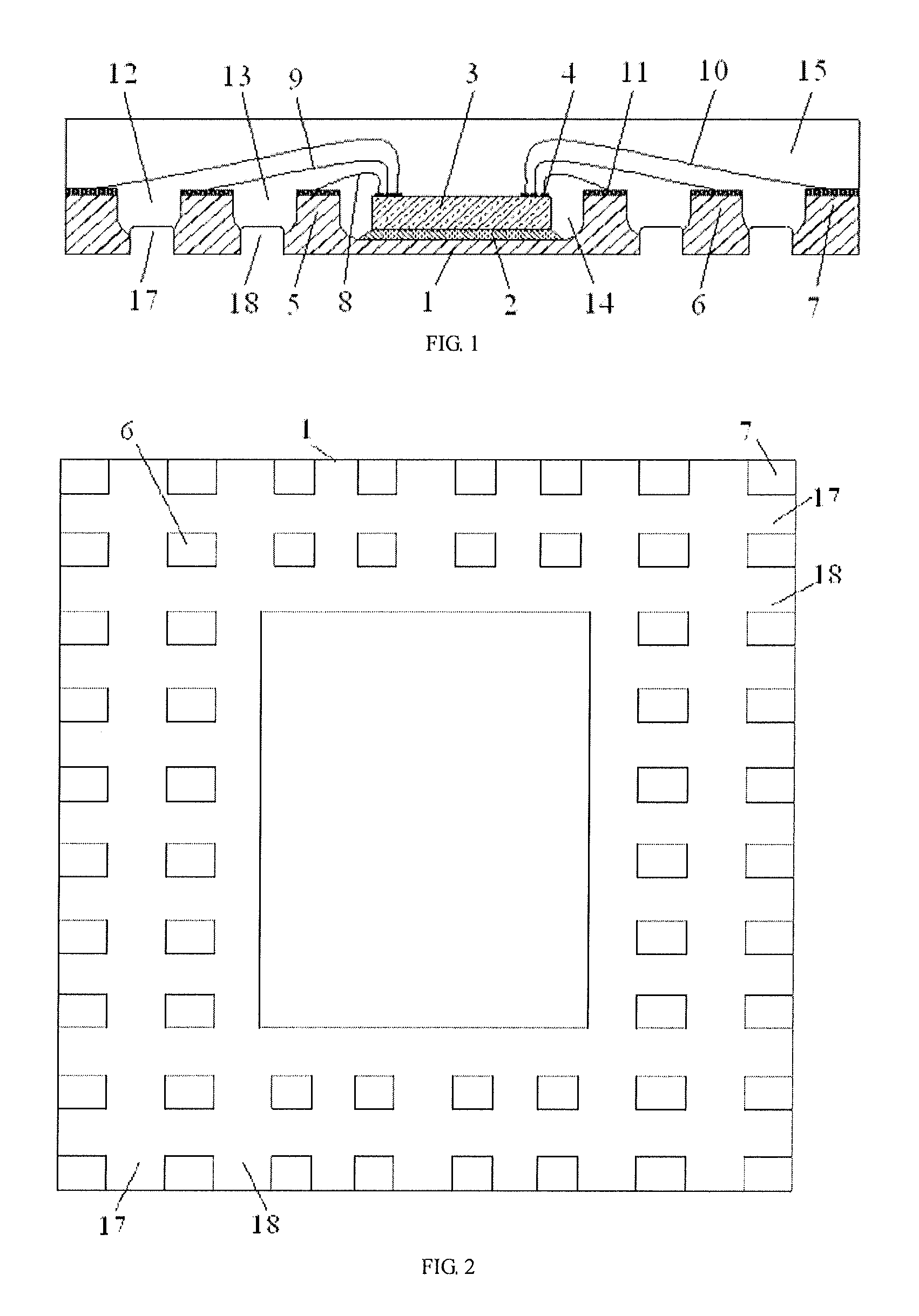
[0107]Adopt an ordinary QFN thinning method to thin a wafer to obtain a wafer having a final thickness of 200 μm, wherein a rough polishing range is from original wafer+adhesive film thickness to 250 μm+adhesive film thickness, a rough polishing speed is 6 μm / s, a fine grinding thickness range is from 250 μm+adhesive film thickness to 200 μm+adhesive film thickness, and a fine grinding speed is 20 μm / min. Adopt a breakage-proof process and adopt a double blade scribing machine to perform scribing on the thinned wafer to obtain an IC chip 3, wherein a breakage-proof and anti-cracking scribing process software control technique is adopted, and a scribing feeding speed is ≦10 mm / s.

[0108]Manufacture a Lead Frame.

[0109]First step: take a copper plate having a thickness of 8 mil, and pretreat the surface of the copper plate including degreasing, micro corrosion, pickling and washing, removing oil stain, fingerprints and oxides on the surface of the copper plate, and coarsening the surface...

embodiment 3

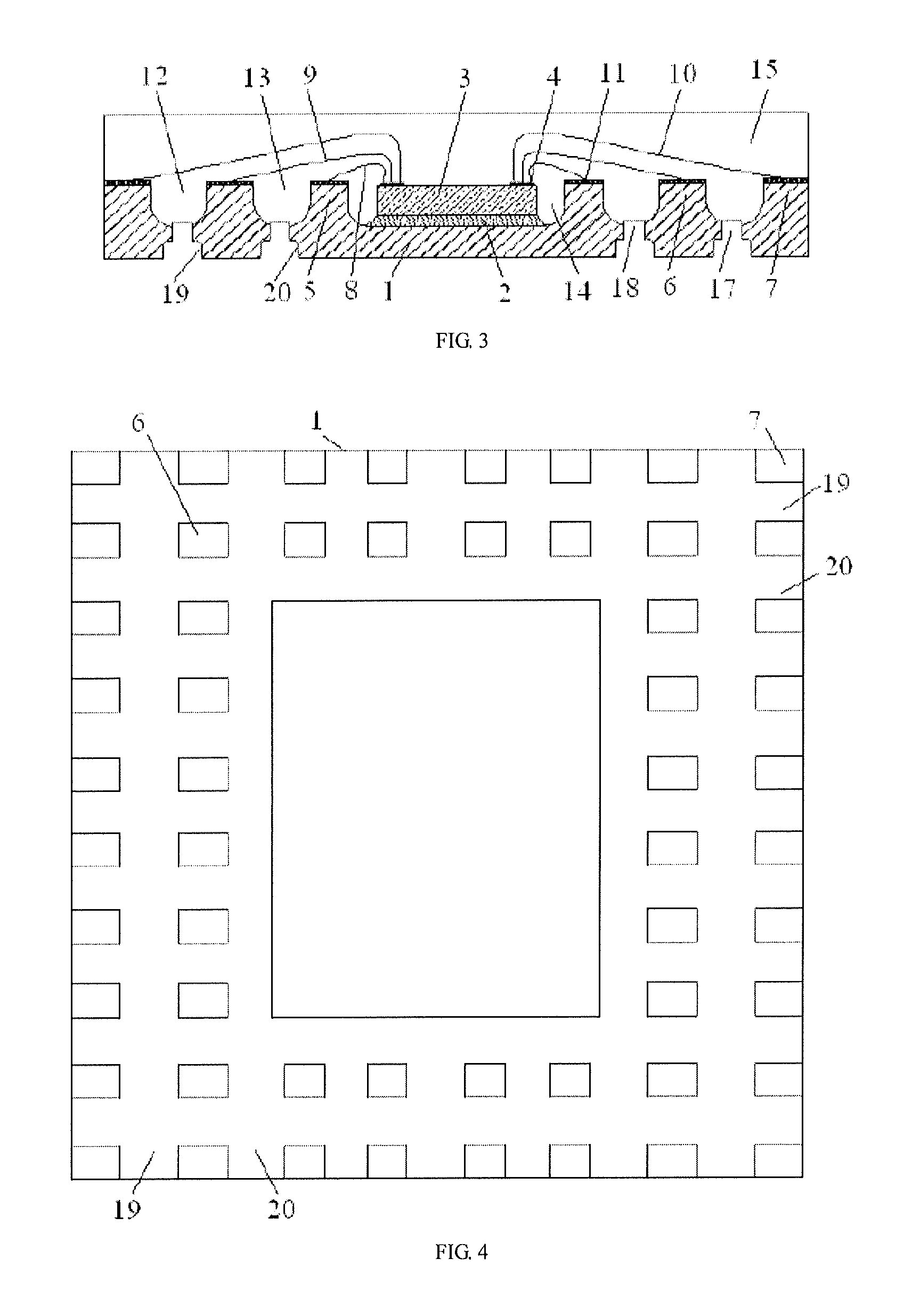
[0117]Adopt an ordinary QFN thinning method to thin a wafer to obtain a wafer having a final thickness of 175 μm, wherein a rough polishing range is from original wafer+adhesive film thickness to 225 μm+adhesive film thickness, a rough polishing speed is 4.5 m / s, a fine grinding thickness range is from 225 μm+adhesive film thickness to 175 μm+adhesive film thickness, and a fine grinding speed is 15 μm / min. Adopt a breakage-proof process and adopt an A-WD-300TXB scribing machine to perform scribing on the thinned wafer to obtain an IC chip 3, wherein a breakage-proof and anti-cracking scribing process software control technique is adopted, and a scribing feeding speed is ≦10 mm / s.

[0118]Manufacture a Lead Frame.

[0119]First step: take a copper plate having a thickness of 7 mil, and pretreat the surface of the copper plate including degreasing, micro corrosion, pickling and washing, removing oil stain, fingerprints and oxides on the surface of the copper plate, and coarsening the surfac...


PUM


Abstract

The present invention discloses a quad flat no lead package and a production method thereof. The quad flat no lead package comprises a lead frame carrier consisting of a carrier pit and three circles of leads arranged around the carrier pit, wherein the three circles of leads respectively consist of a plurality of leads that are disconnected mutually; an IC chip is adhered in the carrier pit; and an inner lead chemical nickel and porpezite plated layer is plated on all the leads; the inner lead chemical nickel and porpezite plated layer is arranged in the same direction as the IC chip; the IC chip is connected with the inner lead chemical nickel and porpezite plated layer through a bonding wire; and the IC chip, the ends of all the leads plated with the inner lead chemical plating nickel and palladium metal layers and the bonding wire are all packaged in a plastic package. The quad flat no lead package is manufactured through the following steps of: thinning and scribing a wafer; manufacturing a lead frame; loading the chip; performing pressure welding and plastic packaging; performing post-curing; printing; electroplating; separating the leads; separating a product; and testing / braiding. According to the package, the problems of few leads, long welding wire, high welding cost and limited frequency application during single-face packaging of the existing normal quad flat no lead package are solved.

Description

FIELD OF THE INVENTION[0001]The present invention belongs to the field of electronic information automation component and part manufacturing technology, and relates to a quad flat no lead package. The present invention further relates to a production method of the package.BACKGROUND OF THE INVENTION[0002]In recent years, with the rapid development of convenient electronic components and parts in the field of mobile communication and mobile computer, small packaging and high-density assembly technologies have been considerably developed. Meanwhile, a series of rigor requirements are raised on the small packaging technology, for example, the packaging size is required as small as possible (particularly, the packaging height is smaller than smaller than 1 mm). The connection reliability after packaging shall be improved as much as possible so as to adapt to lead-free welding (protect the environment) and effectively reduce the cost.[0003]For a long time, a single circle lead frame mode...

Claims


Application Information

Patent Timeline
Patent Type & Authority Patents(United States)
IPC IPC(8): H01L21/00H01L21/48H01L23/495H01L23/31H01L23/00
CPCH01L23/49524H01L21/4832H01L23/3107H01L23/49541H01L23/49579H01L24/03H01L24/29H01L24/45H01L23/49582H01L2224/0311H01L2224/0381H01L2224/03614H01L2224/29155H01L2224/32245H01L2224/43847H01L2224/4502H01L2224/45147H01L2224/48247H01L2224/48257H01L2224/73265H01L2924/00012H01L2924/00H01L23/3121H01L2224/83855H01L2924/00014H01L2224/85464H01L2224/85455H01L2224/2919H01L2224/2929H01L2224/293H01L2924/181H01L24/48H01L24/85H01L2224/85181H01L2224/48091H01L2224/32257H01L2924/12042H01L24/73H01L2224/49433H01L2224/43
Inventor ZHU, WENHUIMU, WEIXU, ZHAOMINGGUO, XIAOWEI
Owner TIANSHUI HUATIAN TECH
Why Eureka
Try Eureka