

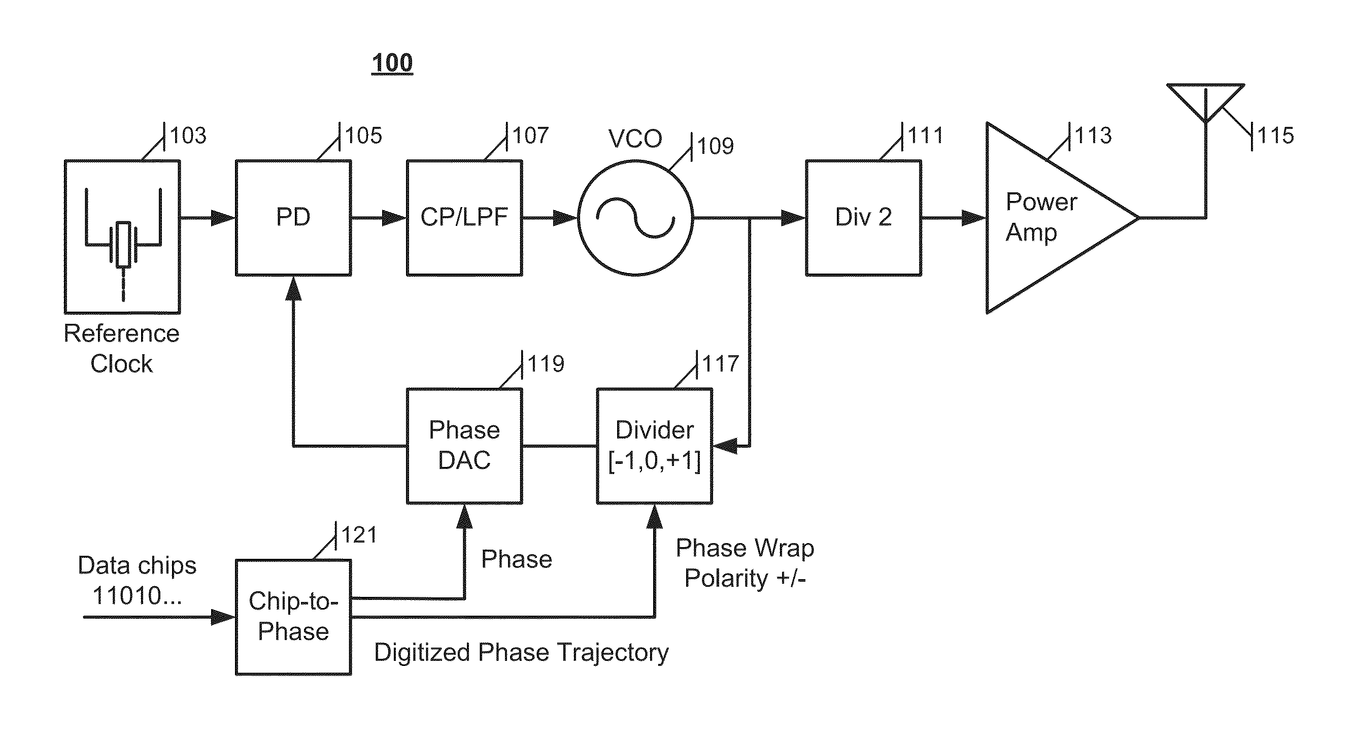
Arbitrary phase trajectory frequency synthesizer
a frequency synthesizer and phase trajectory technology, applied in the direction of pulse generator, electric pulse generator circuit, pulse automatic control, etc., can solve the problems of increasing the delay of digitally adjustable phase dac of the digital signal converter, increasing the digitally adjustable delay of the phase dac, and many radio architectures that are not compatible with lower power supply voltages and reduced headroom voltages
- Summary
- Abstract
- Description
- Claims
- Application Information
AI Technical Summary
Benefits of technology
Problems solved by technology
Method used
Image

Examples
case 1
[0085] IEEE 802.15.4 OQPSK at 2 Mchip / sec
[0086]The IEEE 802.15.4 standard uses OQPSK with half-sine pulse shaping modulation with sixteen 5 MHz-spaced channel centers between 2.405 to 2.48 GHz. Through a mathematical transformation, OQPSK with half-sine pulse shaping can be translated into MSK which is a special case of frequency shift keying (FSK). The modulation uses a higher frequency for 1's and a lower frequency for 0's. Phase is the time integral of frequency, so the phase trajectory is a sequence of ascending or descending ramps. The simplest approach would be to have 1's ramping up and 0's ramping down piecewise. However, a better approach is to use chip pairs (00, 01, 10, 11) instead because an optimum trajectory shape can be chosen for the phase reversals (01 and 10).
[0087]FIG. 10 shows results from a IEEE 802.15.4 simulation with an initial phase locking transient (between 0 and 0.1 usec) followed by phase trajectory tracking of a chip sequence [0,0,0,1,0,1,0,0,0,1,1,1,1,...
case 2
[0088] GMSK at 4 Mchip / sec
[0089]The proposed transmitter can modulate signals at higher chip rates and provide an arbitrary level of Gaussian smoothing. FIG. 13 shows a trajectory with 4 Mchip / sec GMSK with a modulation index of 0.5 and BT=0.5 (BT is a measure of Gaussian smoothing). The Gaussian shaped GMSK is shown relative to MSK phase in FIG. 13. FIG. 14 shows the simulated power spectrum at 8 dBm. The controller bandwidth was 2 MHz for this simulation. Because GMSK is more spectrally efficient, the GMSK 4 Mchip / sec signal has about the same channel width as the half rate IEEE 802.15.4 2 Mchip / sec channel width. Hence, twice the data rate can be transmitted in the same bandwidth.
case 3
[0090] Bluetooth Classic at 1 Mchip / sec
[0091]The final simulation example is for Bluetooth classic. This is GFSK with 1 Mchip / sec, modulation index of 0.32, and a Gaussian smoothing BT=0.5. The charge pump currents were reduced to provide a PLL loop bandwidth of 0.5 MHz to smooth the phase DAC quantization error for the slower signals. The low PLL loop bandwidth will also smooth any sub-LSB (least-significant bit) interpolation of the DAC levels using dithering (e.g., alternating between two adjacent DAC codes via pulse code modulation, or delta sigma modulation, at a rate higher than the desired signal bandwidth to attain a finer in-band signal resolution than the DAC provides alone). The disadvantage of a lower PLL loop bandwidth is increased phase noise since the PLL will not attenuate as much noise power. FIG. 15 shows the Bluetooth trajectory, and FIG. 16 shows the narrow 1 MHz channel power spectrum at 8 dBm.
[0092]The transmitters 100-600 shown in and described in relation to ...
PUM
 Abstract
Description
Claims
Application Information