Hermetically sealed package having stress reducing layer

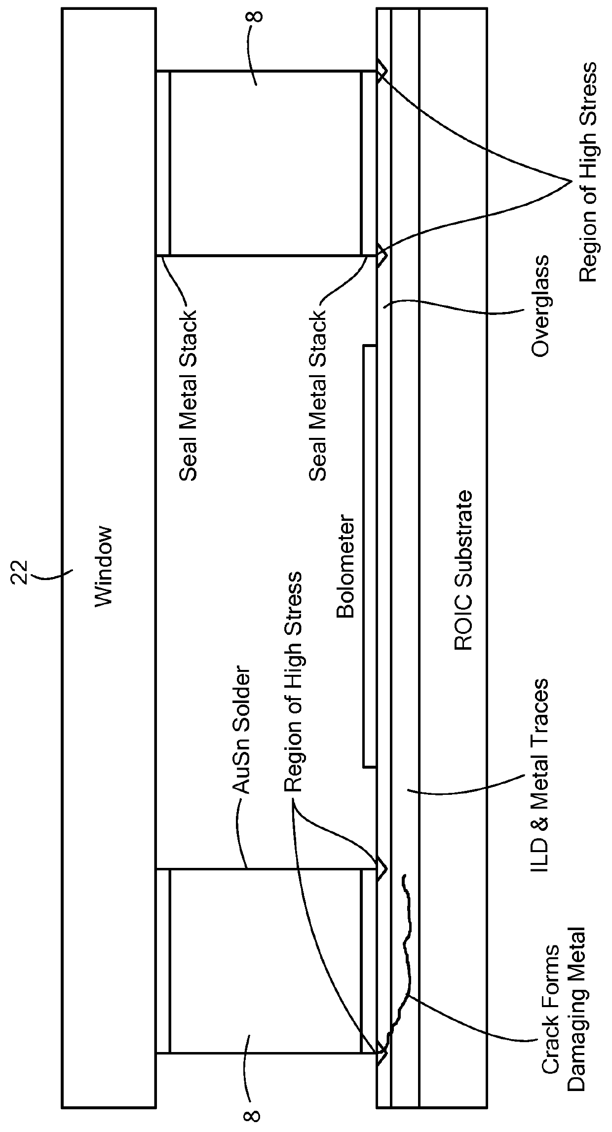
a technology of stress reduction layer and hermetically sealed package, which is applied in the field of microelectromechanical system (mems) packaging, can solve the problems of shrinking solder layer, unwanted cracks in the overglass and underlying structure of the device or roic, and the cost of packaging mems devices in traditional metal or ceramic package may be on the order of 10 to 100 times the device fabrication cost, etc., to achieve high stress, high ductility, and high thermal contraction ra

Active Publication Date: 2016-05-10
RAYTHEON CO
View PDF18 Cites 2 Cited by
  • Summary
  • Abstract
  • Description
  • Claims
  • Application Information

AI Technical Summary

Benefits of technology

[0005]As is the case with certain microelectromechanical (MEMS) devices, bolometers may need to be hermetically packaged in vacuum or other controlled environment conditions for best performance. Exemplary requirements for the packaging of bolometer arrays include reliable hermetic sealing capable of maintaining a high vacuum for an extended period of time, the integration of IR window material with good infrared transmission, and high yield / low cost packaging. Both the reliability and the cost of MEMS devices depend upon encapsulation (packaging) techniques chosen. For MEMS based bolometers, packaging may be done at the chip level or at the wafer level. A common way of packaging in this instance is to fabricate a protective, IR-transmitting cap wafer, or Window Cap Wafer (WCW), and bond it to an exposed surface of the semiconductor substrate, or device wafer, containing the active IR detector bolometer areas prior to dicing. The cap wafer, sometimes, also referred to as a window or lid structure, is formed with cavities therein such that when the cap wafer is flipped and bonded to the device wafer, the cavities provide sufficient clearance to accommodate and protect the MEMS devices therein as described in U.S. Pat. No. 5,701,008, entitled Integrated infrared microlens and gas molecule getter grating in a vacuum package, inventors Ray et al., issued Dec. 23, 1997. As described therein, and referring to FIGS. 1 and 2, a package assembly is shown having a readout integrated circuit (ROIC) substrate 2 of a semiconductor material, preferably silicon. An IR detector array 14 is positioned on the substrate 2 and includes a plurality of individual detector elements, also called pixels, 6. Although FIG. 2 shows only a 5×6 rectangular array of detector pixels 6 in detector region 10, it is understood that a typical IR integrated circuit generally includes a planar IR detector array with up to several hundred or even thousand by several hundred or even thousand pixels 6. In most commercial applications, IR detectors are usually uncooled and detect the intensity of IR radiation by sensing increases in temperature which result from the heat imparted to the detectors by the IR radiation. A typical example of an uncooled IR detector is a vanadium oxide (VOx) microbolometer (MB), in which a plurality of individual detectors are usually formed in an array on the ROIC substrate 2 by conventional semiconductor manufacturing processes. The MB array detects IR radiation by sensing the IR-generated heat, and is also called a focal plane array (FPA) or a sensor chip assembly (SCA). The substrate 2 is an integrated circuit used to process the signal produced by the bolometers. In this case the bolometer is a microbridge resistor that changes its resistance when its temperature changes. The incoming radiation causes a change in the temperature of the microbridge. Although other semiconductor materials such as Si may be used, VOx is a commonly available and cost effective material that is used in most commercial IR detection applications.
[0009]More particularly, the inventors have recognized that in the prior art the seal ring metal stack (about 0.5 um thick) and the solder (up to 11 um thick) have a coincident edge. As the solder cools below its ˜280 degree Centigrade melting temperature the solder shrinks faster than the underlying seal ring and ROIC (solder CTE ˜16 ppm, silicon CTE ˜3 ppm), and the solder is very stiff (AuSn solder has a high Young's modulus) so it cannot deform to relieve the stress. The shrinkage of the solder layer tends to pull on the edge of the solder joint, which is the source of a stress point r and the resulting crack at the edge of the joint. Simply increasing the thickness of the titanium (Ti) portion of the underlying portion of the seal ring has little effect on stress because one is still left with the solder pulling on the edge of the seal ring, which results in the stress point. By terminating the solder short of the edge of the metal that adheres to the ROIC surface and providing an intervening layer, the stress relief buffer layer, of, for example, titanium, the abrupt edge that conducts the stress down to a localized region on the ROIC surface is terminated above the ROIC's surface and covered with a more ductile material. The inventers have further recognized that once the coincident edge is eliminated, thickening the underlying titanium layer either by thickening the stress relief buffer layer, in one embodiment, or thickening the titanium bonding material adhesion layer, in another embodiment, will further reduce stress, but only if the coincident edge is first eliminated.
[0019]More particularly, when using a solder having a high thermal contraction rate to bond and hermetically seal the two wafers to form the package, as the solder cools from it's melted temperature it shrinks, inducing high levels of stress in the underlying semiconductor wafer at the edges of the solder joint. The use of the stress relief buffer layer 1 isolates the high stress region at the edge of the solder joint from the underlying brittle semiconductor wafer, interposing the material of the stress relief buffer layer having a higher level of ductility than the ductility of the semiconductor wafer, and a thermal contraction rate less than the solder yet higher than the underlying wafer. The stress relief buffer layer has a thermal expansion between that of the solder layer and the surface of the wafer and reduces the stress in the more brittle wafer. Thus, the disclosure enables the integration of a high CTE solder or other bonding material with a brittle overglass layer on a semiconductor structure. Further, the process may be used on the device wafer, lid or both.

Problems solved by technology

Often, however, the cost of packaging MEMS devices in traditional metal or ceramic packages may be on the order of about 10 to 100 times the device fabrication cost.
These stresses may cause unwanted cracks to develop in the overglass and underlying structure of the device or ROIC wafer as shown in FIG. 3.
These cracks can break the interlayered dielectric layer (ILD) and metal interconnecting traces in the ILD of the ROIC leading to failure.
The shrinkage of the solder layer tends to pull on the edge of the solder joint, which is the source of a stress point r and the resulting crack at the edge of the joint.
More particularly, when using a solder having a high thermal contraction rate to bond and hermetically seal the two wafers to form the package, as the solder cools from it's melted temperature it shrinks, inducing high levels of stress in the underlying semiconductor wafer at the edges of the solder joint.

Method used


Image

  • Hermetically sealed package having stress reducing layer
  • Hermetically sealed package having stress reducing layer
  • Hermetically sealed package having stress reducing layer

Examples


Embodiment Construction

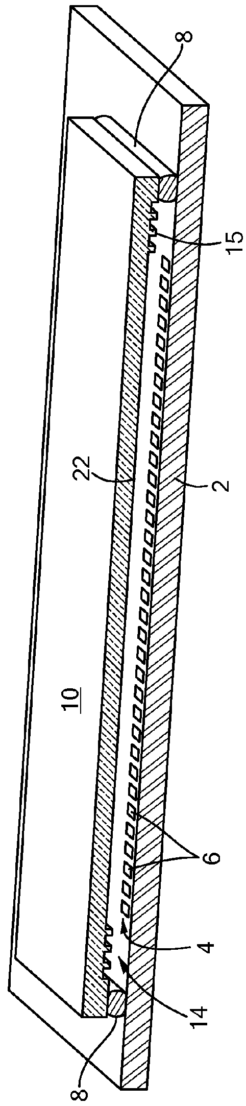
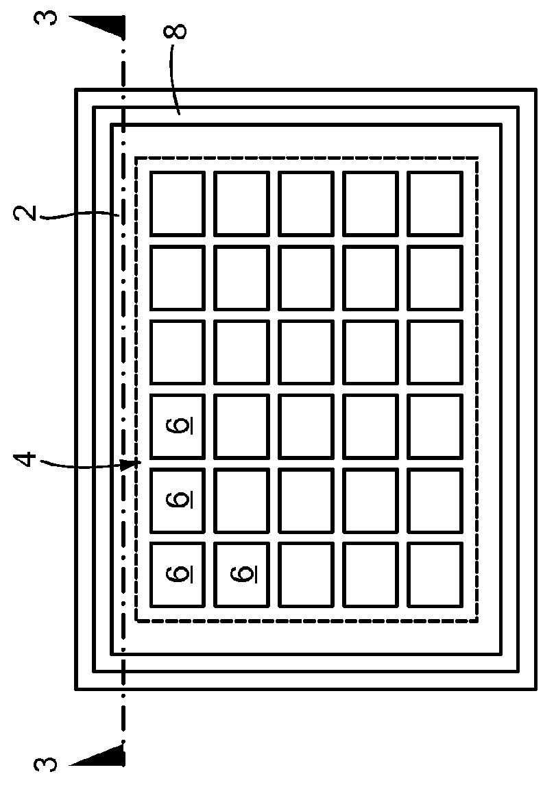
[0031]Referring now to FIGS. 4 and 5, a hermetically sealed package 100 is shown for hermetically sealing a device 102. The package 100 includes: substrate 104 having, in a central region 106 thereof, the device 102; a cap wafer 108 (FIG. 5); and a pair of metal rings, here for example, multi-layer metal rings, 107DW metal ring, 107CW; metal ring 107DW being disposed on a surface of the substrate 104 around a surface region 106 of the substrate 104, and the other metal ring 107CW being disposed on the surface of the cap wafer 108 around the central region 106. It should be understood that in some applications the metal ring 107CW may not be needed. The metal ring 107DW includes: a ring-shaped stress relief buffer layer 109DW disposed on, and in direct contact with, the surface of the substrate 104 (more particularly on and in direct contact with an overglass layer 116 of the substrate 104), as shown more clearly in FIG. 5A; and a seal ring structure 110DW (FIG. 5), on the upper surf...


PUM


Abstract

A sealed package having a device disposed on a wafer structure and a lid structure boned to the device wafer. The device wafer includes: a substrate; a metal ring disposed on a surface portion of substrate around the device and a bonding material disposed on the metal ring. The metal ring extends laterally beyond at least one of an inner and outer edge of the bonding material. A first layer of the metal ring includes a stress relief buffer layer having a higher ductility than that of the surface portion of the substrate and a width greater than the width of the bonding material. The metal ring extends laterally beyond at least one of the inner and outer edges of the bonding material. The stress relief buffer layer has a coefficient of thermal expansion greater than the coefficient of expansion of the surface portion of the substrate and less than the coefficient of expansion of the bonding material.

Description

TECHNICAL FIELD[0001]This disclosure relates generally to electronic packaging and more particularly to Microelectromechanical system (MEMS) packaging.BACKGROUND AND SUMMARY[0002]As is known in the art, Microelectromechanical systems (MEMS) are integrated micro devices or systems combining electrical and mechanical components. MEMS devices may be fabricated using, for example, standard integrated circuit batch processing techniques. Exemplary applications for MEMS devices include sensing, controlling, and actuating on the micro scale. Such MEMS devices may function individually or in arrays to generate effects on a macro scale.[0003]As is also known in the art, many MEMS devices require a hermetically sealed environment in order to attain maximum performance. This could be a vacuum environment, a controlled pressure environment or a controlled gas environment. The package environment also provides protection and an optimal operating environment for the MEMS device. Specific examples...

Claims


Application Information

Patent Timeline
Patent Type & Authority Patents(United States)
IPC IPC(8): H01L23/552B81B7/00
CPCB81B7/0048B81B2201/0207B81C2203/035B81B7/0051B81C1/00333B81C1/00825
Inventor KENNEDY, ADAM M.DIEP, BUU Q.BLACK, STEPHEN H.WONG, TSE E.KOCIAN, THOMAS ALLANTRACY, GREGORY D.
Owner RAYTHEON CO
Why Eureka
Try Eureka