

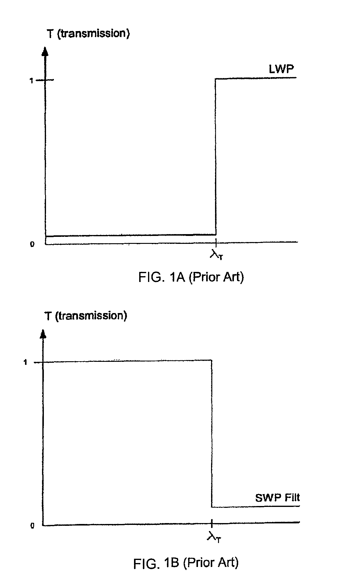
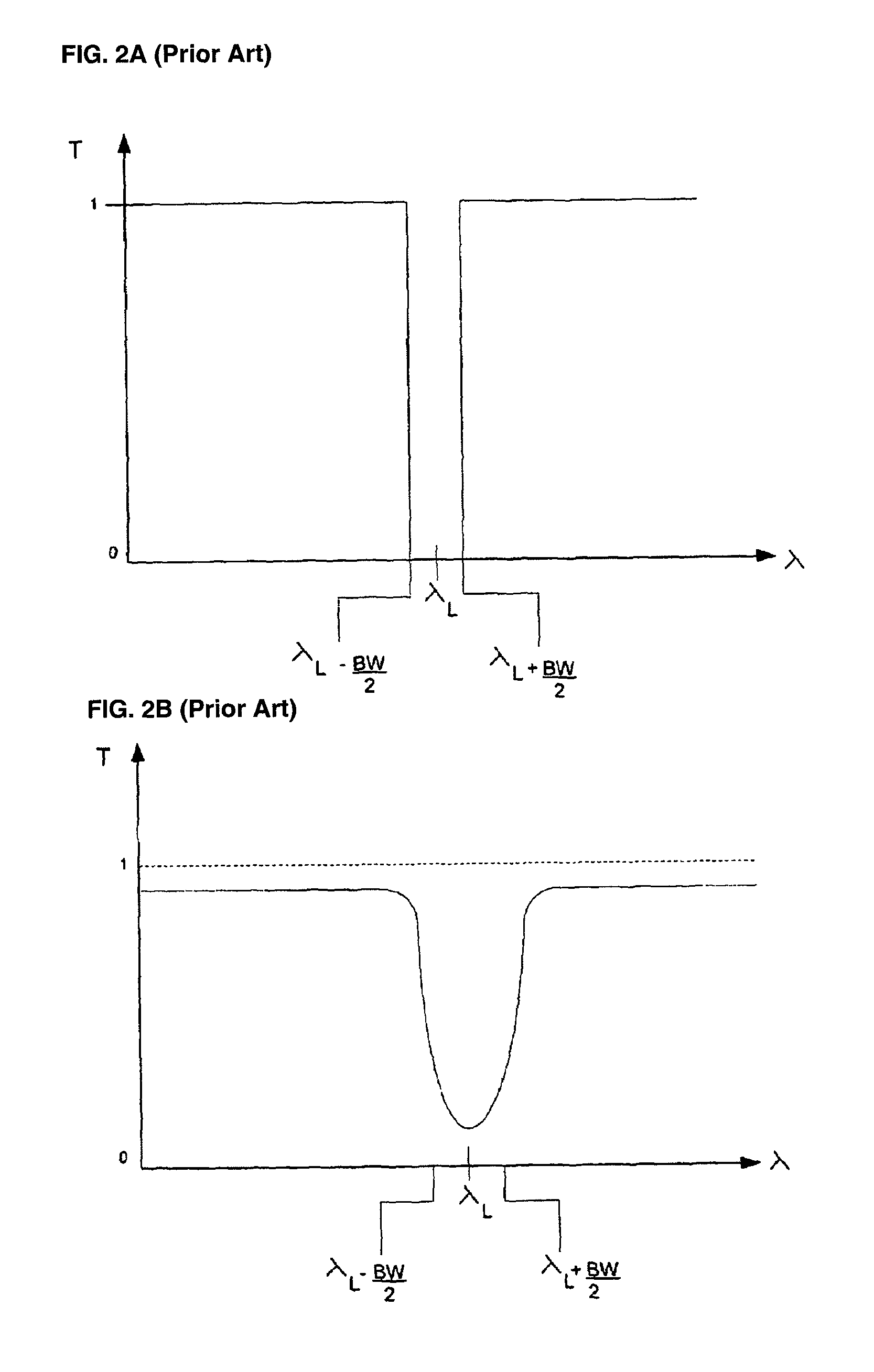
Optical thin-film notch filter with very wide pass band regions
a very wide pass band technology, applied in the field of optical thin film notch filter with very wide pass band, can solve the problems of eroded performance of the system in which they are utilized, real filters have some amount of transmission loss, real notch filters do not perfectly transmit light outside of the notch band, etc., to achieve the effect of improving resistance to material variation
- Summary
- Abstract
- Description
- Claims
- Application Information
AI Technical Summary
Benefits of technology
Problems solved by technology
Method used
Image

Examples
examples 1-3
Thin Film Notch Filter Designs Based on SWP or LWP Pass Band Defect
[0129]Three filter designs (filters 300m, 400m, 500m) in accordance with the present disclosure were produced by optimizing a standard SWP or LWP edge filter design having an initial structure corresponding to (0.5H:L:0.5H)N, where H and L are quarter wave thick layers of materials having high and low refractive index, respectively, and N is an integer determined by coating thickness. The initial design was optimized against a design spectrum using well-known optimization algorithms (e.g., the variable metric approach) to produce a design spectrum for a thin film notch filter comprising two materials and exhibiting a SWP pass band defect (i.e., filter 300m), a notch filter comprising two materials and exhibiting a LWP pass band defect (i.e. filter 400m), and a notch filter comprising three materials and exhibiting a SWP pass band defect and (i.e., filter 500m). For the third design (500m), the high and low index mate...
example 4
Single Notch Filter Based on Pass Band Defect and Exhibiting Extended Pass Band Bandwidth
[0139]A thin film notch filter 600m based on LWP pass band defect was designed having the configuration shown in the following table.
[0140]
TABLE 2Notch Filter (600 m) Having A Single Notch at 632.8 nm.Layer #MaterialThickness (nm)Layer #MaterialThickness (nm)1Ta2O510.002SiO268.153Ta2O517.694SiO257.855Ta2O528.526SiO242.207Ta2O536.008SiO242.449Ta2O534.2210SiO243.4311Ta2O532.5012SiO252.9613Ta2O525.5314SiO256.7215Ta2O527.2116SiO254.7417Ta2O525.9518SiO252.0319Ta2O531.4720SiO243.3621Ta2O530.6622SiO248.1423Ta2O529.5524SiO244.9725Ta2O528.9326SiO253.1327Ta2O525.0028SiO250.9329Ta2O529.2630SiO249.9431Ta2O526.9332SiO249.9033Ta2O531.7734SiO243.9935Ta2O529.0436SiO251.2337Ta2O528.3538SiO245.3139Ta2O528.4840SiO252.5841Ta2O524.8942SiO247.7643Ta2O530.2644SiO246.6345Ta2O526.5346SiO249.3147Ta2O530.6748SiO243.3249Ta2O528.2550SiO252.3351Ta2O527.0352SiO245.1753Ta2O529.2054SiO251.4955Ta2O525.0156SiO247.5757Ta2O531.4158...
examples 5 and 6
Fabricated Single Notch Filters Based on Pass Band Defect and Exhibiting Extended Pass Band Bandwidth
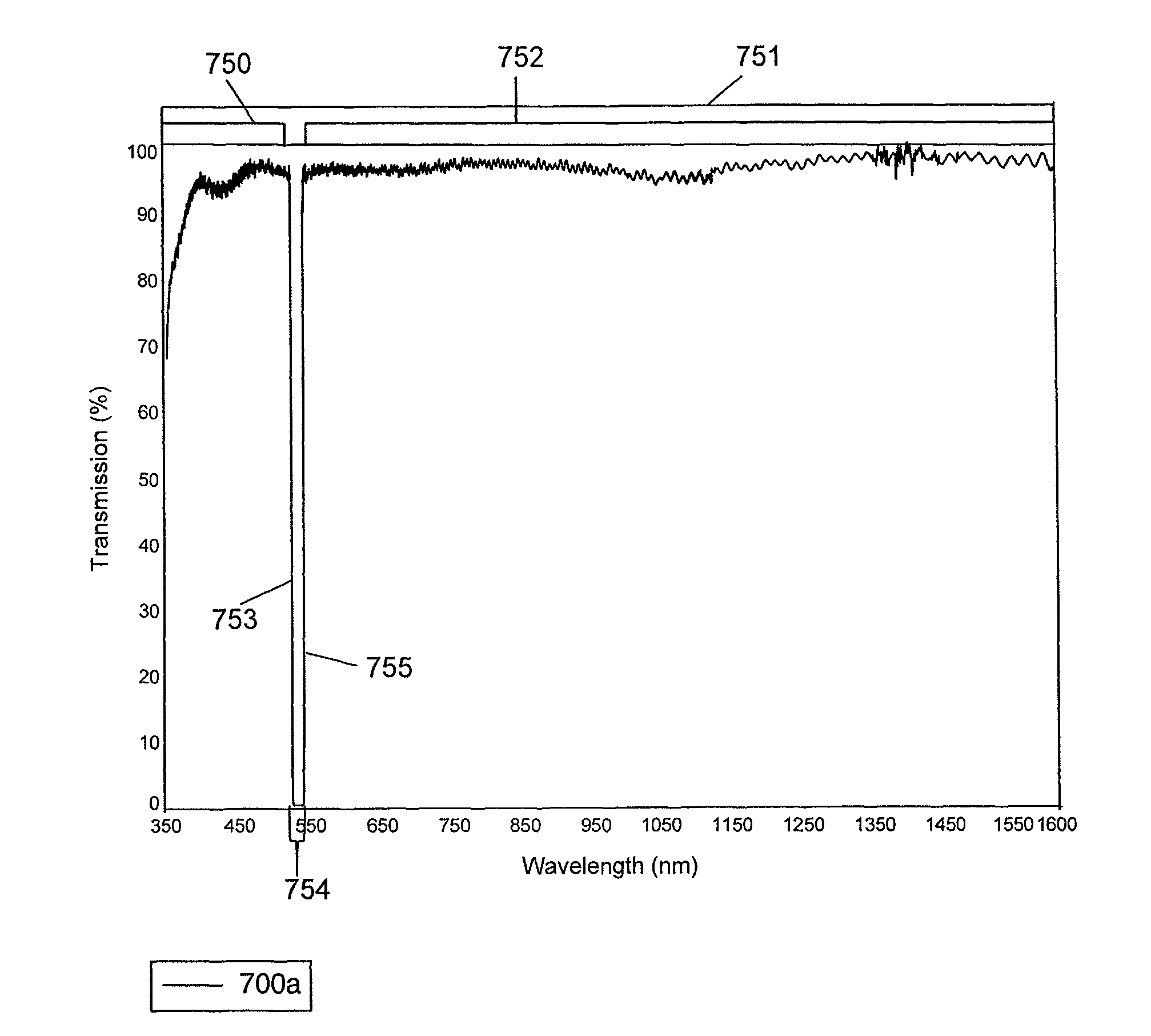
[0144]Two thin film notch filters (700m, 800m) based on LWP pass band defect were designed having the configurations shown in the following table.
[0145]
TABLE 3Notch filters based on LWP pass band defectExample 5:Example 6:Single Notch Single Notchat 532 nmat 808 nmLayer(700 m)(800 m)No.MaterialLayer thickness in nm1Ta2O51010.0038232SiO265.80105365.1504973Ta2O520.24587619.2629964SiO249.72427554.2156645Ta2O533.36210928.9059266SiO237.09750842.2785847Ta2O540.98957539.1310718SiO233.89998336.5772229Ta2O540.88215537.09156910SiO240.52006245.89546811Ta2O532.45060930.42245912SiO251.23294852.74596313Ta2O527.46329928.01382514SiO259.34817 57.94593115Ta2O524.74709424.61788116SiO255.78476261.46210117Ta2O528.75255427.34351718SiO250.093699 49.65382619Ta2O532.070406 34.49910520SiO243.11907945.32016321Ta2O533.8573532.73134322SiO245.106228 49.37700123Ta2O531.76459 32.30405924SiO246.293392 48.01411125Ta2...
PUM
 Abstract
Description
Claims
Application Information