

Selective layer disordering in III-nitrides with a capping layer
a technology of iiinitrides and capping layers, applied in semiconductor devices, lasers, semiconductor lasers, etc., can solve the problems of limited demonstrations to discrete devices, and achieve the effects of slowing down si diffusion, reducing the rate of layer disordering, and increasing the thickness of sinx
- Summary
- Abstract
- Description
- Claims
- Application Information
AI Technical Summary
Benefits of technology
Problems solved by technology
Method used
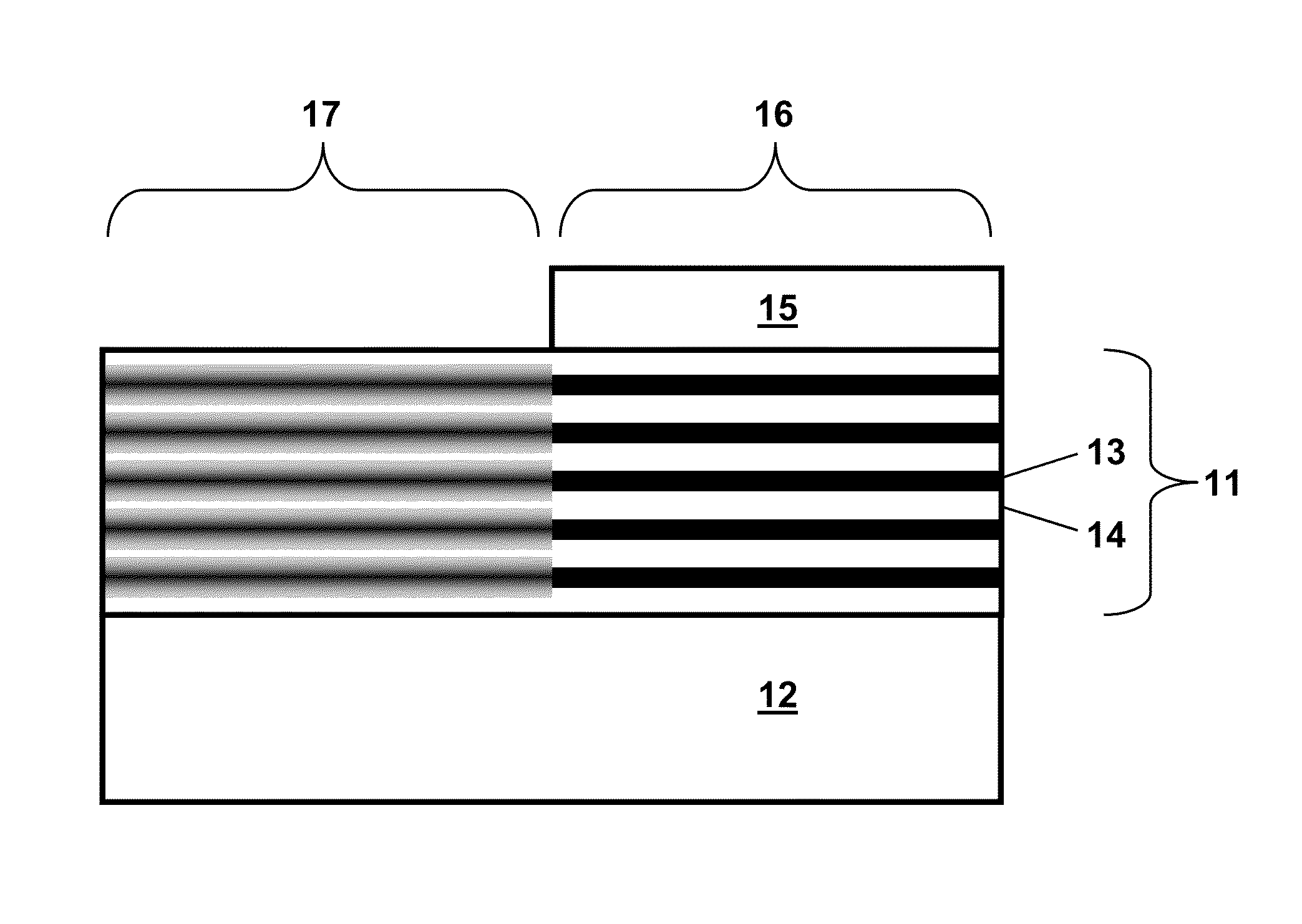
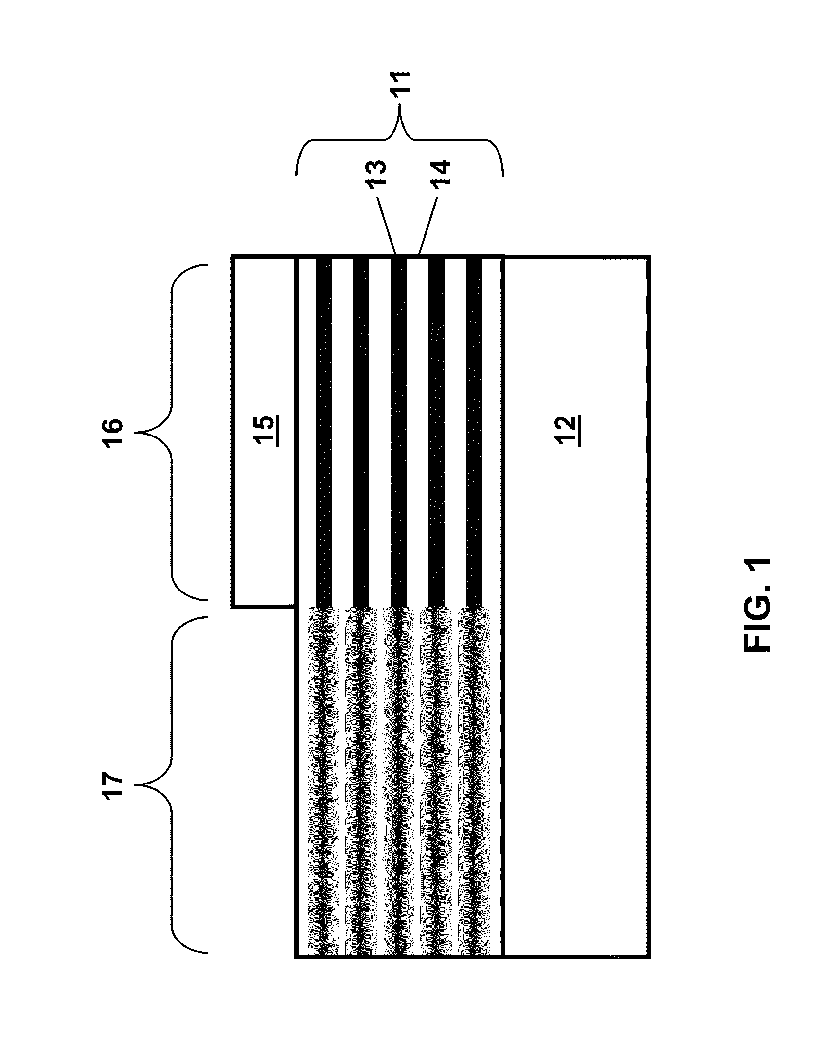
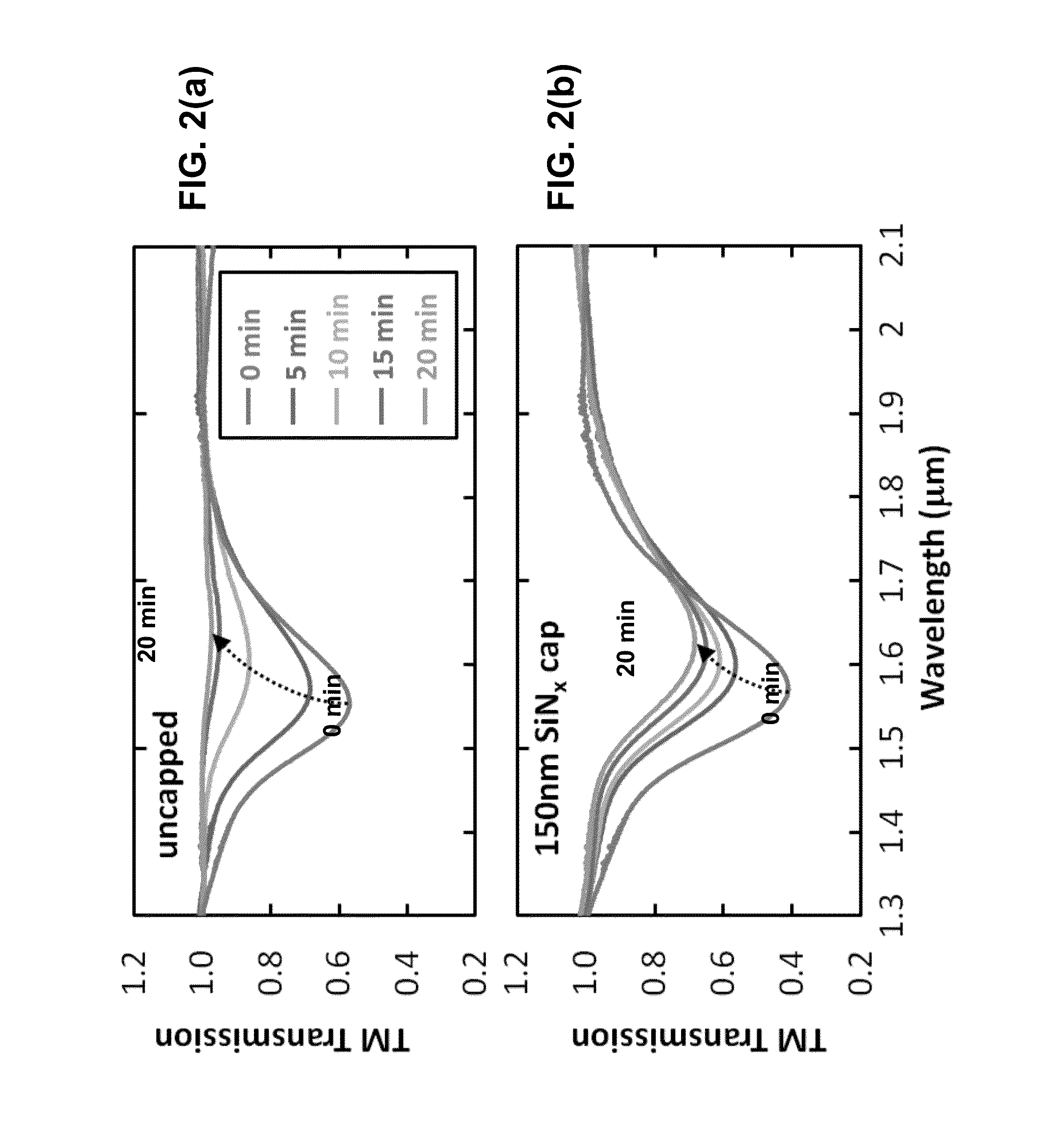
Image

Examples
Embodiment Construction
[0014]A method used in conventional III-V compound semiconductors for device integration is layer disordering. Impurity-induced layer disordering (IILD) or layer intermixing is a well-studied phenomena in the III-arsenide and III-phosphide material systems. See W. D. Ladig et al., Appl. Phys. Lett. 38, 776 (1981); D. G. Deppe and N. Holoyak, Jr., J. Appl. Phys. 64, R93 (1988); and D. G. Deppe et al., Appl. Phys. Lett. 52, 1413 (1988). Normally an unintentionally doped (UID) heterointerface, such as an AlAs / GaAs, is stable (no Al—Ga interdiffusion) up to high temperatures (˜900° C.). See L. L. Chang and A. Koma, Appl. Phys. Lett. 29, 138 (1976). The introduction of impurities by diffusion, implantation, or during growth lowers the temperature where layer disordering can occur. The impurity diffuses at these lower temperatures, and as it travels through the semiconductor layers the crystal atoms can reorganize, leading to intermixing of the heterointerfaces. In particular, movement of...
PUM
 Abstract
Description
Claims
Application Information