Method for manufacturing silicon carbide thin film

a technology of silicon carbide and thin film, which is applied in the direction of coating, chemical vapor deposition coating, plasma technique, etc., can solve the problems of high defect and grain boundary density, not applicable to electronic device applications, and high cost, and achieves good crystallinity, small grain size, and large granular size.

Active Publication Date: 2016-06-21
NATIONAL TSING HUA UNIVERSITY
View PDF2 Cites 17 Cited by
  • Summary
  • Abstract
  • Description
  • Claims
  • Application Information

AI Technical Summary

Benefits of technology

[0011]In the preferred embodiments of the present invention, the precursor containing chlorine atoms may be implemented by dichlorodimethylsilane (DDS) and the precursor not containing chlorine atoms may be implemented by adopting tetramethylsilane (TMS). The SiC thin film fabricated in DDS process has good crystallinity and large gran size, and also has an apparent preferred direction and a columnar-like structure on the sidewall of the film. Although the SiC thin film fabricated in TMS process has small grain size and high grain boundary density as compared to the film obtained by using DDS process, TMS process is an environmentally friendly process and it is also a good option to fabricate the SiC thin film.

Problems solved by technology

This approach causes many problems such as interdiffusion and substrate warping due to different thermal expansion, and therefore the application of this approach is dramatically restricted.
These films have high defect and high grain boundary density, and therefore they are not applicable to electronic device applications.
Therefore, how to solve above problems and manufacturing silicon carbide thin films with high quality at low process temperature are important issues in this industry.

Method used


Image

  • Method for manufacturing silicon carbide thin film
  • Method for manufacturing silicon carbide thin film
  • Method for manufacturing silicon carbide thin film

Examples


Embodiment Construction

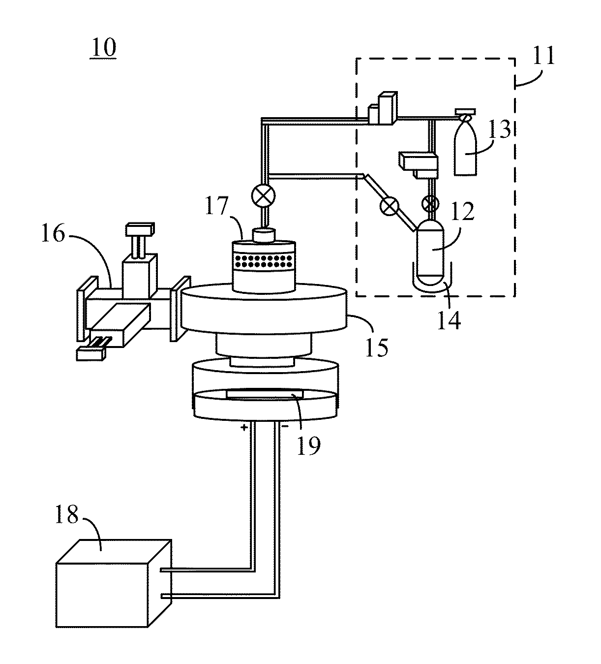
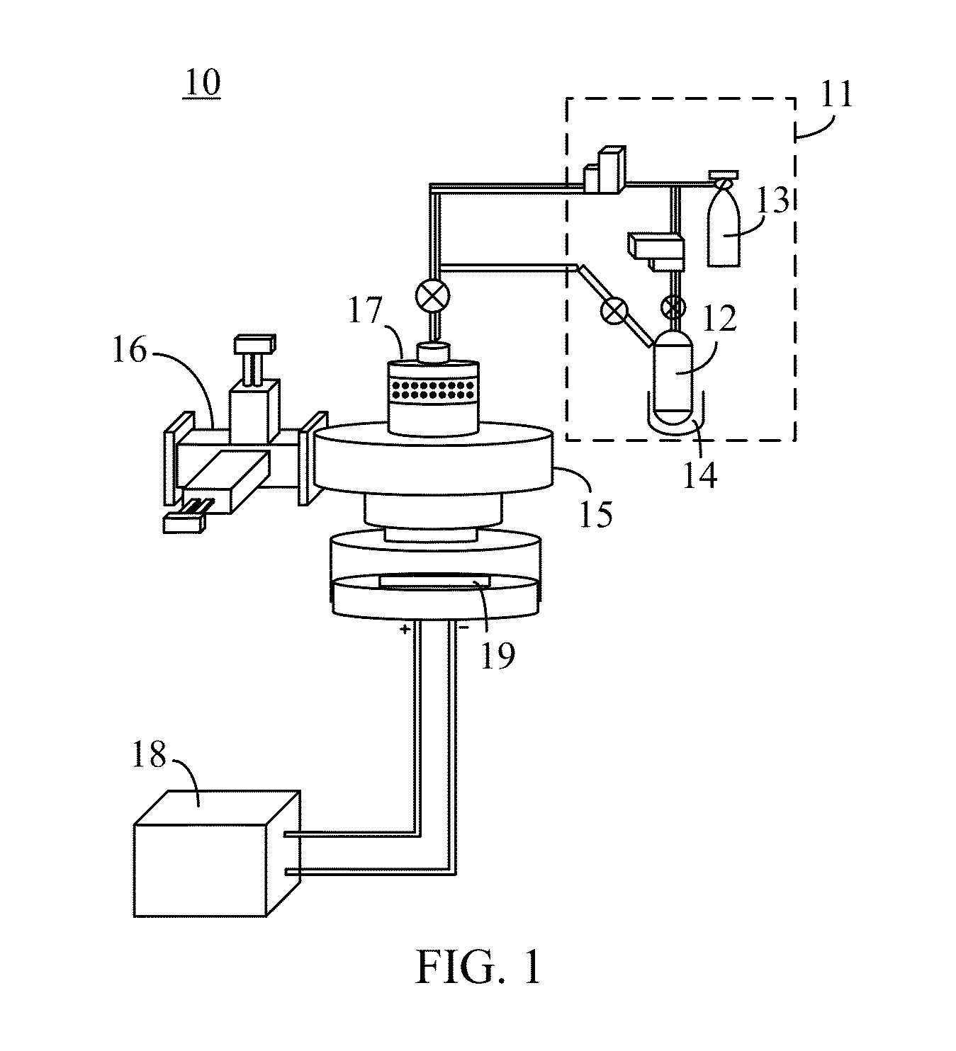
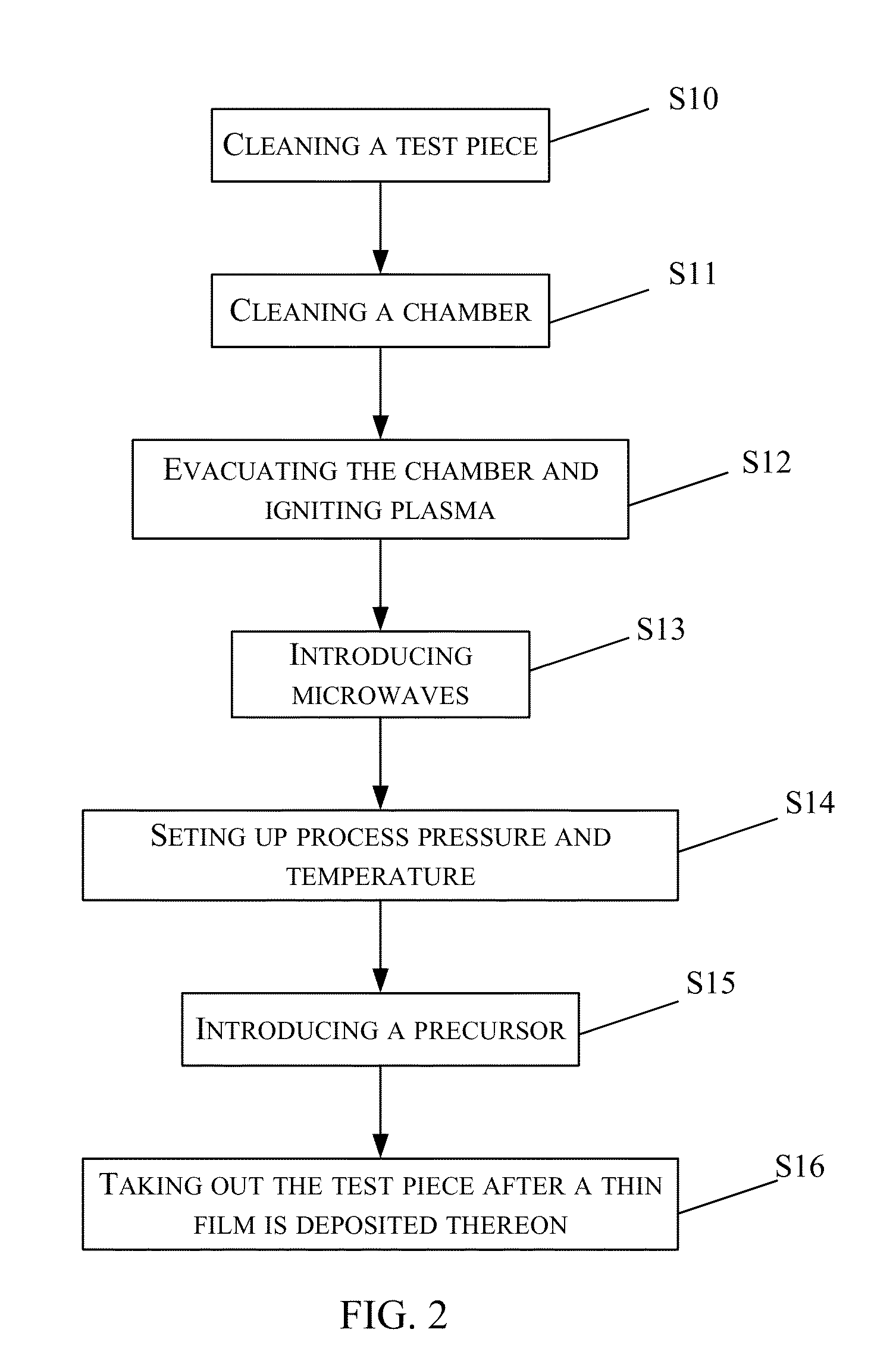
[0020]In the preferred embodiments of the present invention, microwave plasma enhanced chemical vapor deposition (MPECVD) is utilized to grow a silicon carbide (SiC) thin film at low temperature in a low-pressure gas ambience diluting a precursor with a large amount of hydrogen gas. In the present invention, a silicon carbide thin film with good crystallinity can be obtained at a substrate temperature no higher than 400° C. (preferably, 500° C.) under the circumstance of a non-heating process, i.e., without heating the substrate additionally. The low-temperature process greatly increases the range of applications of the silicon carbide thin film, which can be coated on a surface of tool steel, metal, or a glass substrate. The applications of the present invention may range from electronic elements, barrier layers for ion implantation, optoelectronic devices, tool steel, and interposers for growing diamond films to superhard thin films, and they are all applied quite well.

[0021]FIG. ...


PUM

PropertyMeasurementUnit
temperatureaaaaaaaaaa
pressureaaaaaaaaaa
pressureaaaaaaaaaa

Abstract

A method for manufacturing a silicon carbide thin film comprises steps of: (a) utilizing a mechanical pump to remove gases in a chamber such that the pressure in the chamber is reduced to a base pressure; (b) utilizing a microwave generator to generate microwaves at 1200 W to 1400 W so as to form microwave plasma inside the chamber; and (c) introducing into the chamber a silicon-based compound containing chlorine atoms that serve as a precursor, during the time that the temperature of a substrate disposed in the chamber is stable at 400° C. to 500° C., in which the temperature of the substrate is risen by the microwave plasma without heating the substrate additionally, so as to form a film of cubic silicon carbide on the substrate. In the present invention, the SiC thin film has good crystallinity and is manufactured by using MPECVD in a low temperature process.

Description

CROSS REFERENCE[0001]This application claims the priority of Taiwan Patent Application No. 103108163, filed on Mar. 10, 2014.TECHNICAL FIELD OF THE INVENTION[0002]The present invention relates to a method for manufacturing a silicon carbide thin film, and more particularly, to a method for manufacturing a silicon carbide thin film by utilizing microwave plasma enhanced chemical vapor deposition (MPECVD).BACKGROUND OF THE INVENTION[0003]Silicon carbide (SiC) has very excellent physical properties such as high melting point, great hardness, high electron mobility, and high breakdown voltage. Accordingly, silicon carbide is always an important industrial material that is applicable to many technical fields, for example, machinery industry, aerospace industry, and it is also applicable to a great amount of electronic devices. Particularly, silicon carbide plays an important role in those electronic devices with high frequency and high power due to its high electron mobility, high breakd...

Claims


Application Information

Patent Timeline
Patent Type & Authority Patents(United States)
IPC IPC(8): H05H1/30C23C16/44C23C16/32H05H1/24H05H1/46C23C16/511C23C16/02C23C16/455
CPCC23C16/4412C23C16/02C23C16/325C23C16/4405C23C16/4407C23C16/45557C23C16/511
Inventor LEE, CHI-YOUNGCHIU, RU-CHIEN
Owner NATIONAL TSING HUA UNIVERSITY
Why Eureka
Try Eureka