Polycrystalline silicon rod and method for producing polysilicon
a polysilicon and polysilicon technology, applied in the field of polycrystalline silicon preparation, can solve the problems of high production cost of compact rods, increased production costs of compact rods, so as to achieve low production cost and achieve the effect of reducing production costs and avoiding losses in yield and productivity
- Summary
- Abstract
- Description
- Claims
- Application Information
AI Technical Summary
Benefits of technology
Problems solved by technology
Method used
Image
Examples
example 1
Comparative Example
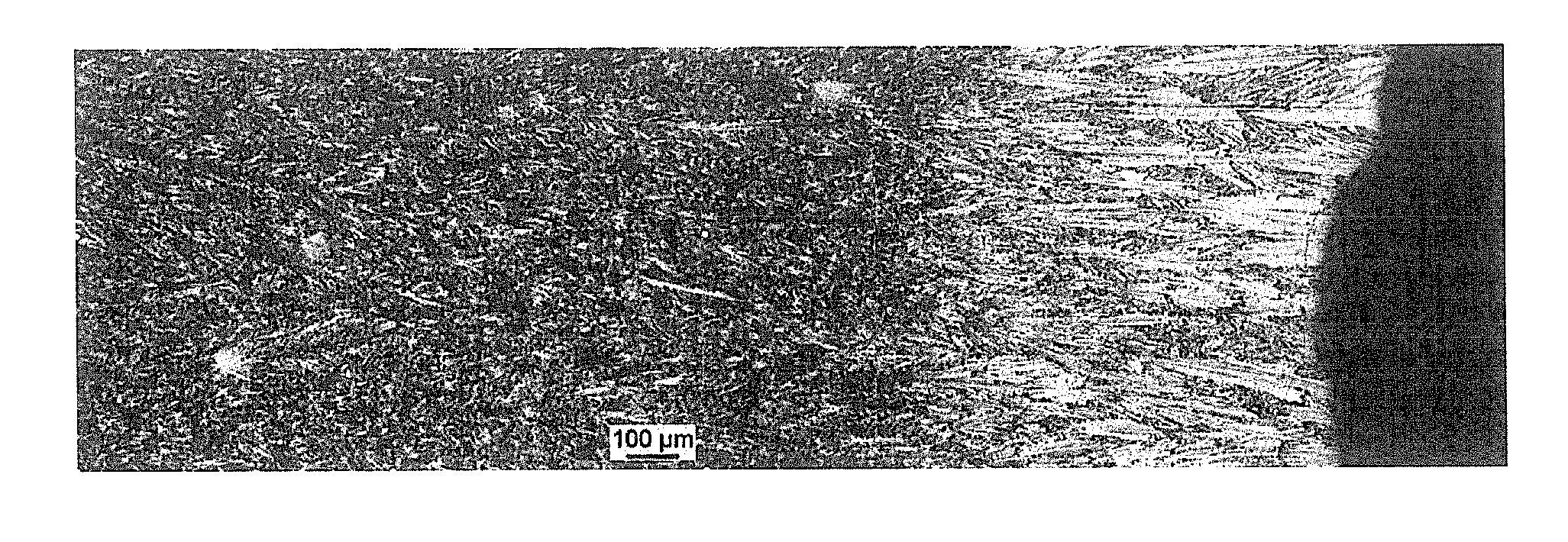
[0070]Compact polycrystalline silicon rods were deposited according to the prior art. The corresponding process is known from US 2010 / 219380 A1. The conditions corresponded to those disclosed in Comparative example 1. The mean crystallite size in the material deposited was about 11 μm. The roughness of the surface Ra was 3.6 μm. Finally, the rods—as described in US2007 / 235574 A1—were broken into chunks. This was followed by a wet-chemical treatment of the chunks, as disclosed in US2010 / 001106 A1. When this material was used in the above-described pulling process, it was possible to achieve a mean yield of 95.4%.
example 2
Comparative Example
[0071]Here too, compact polycrystalline silicon rods were deposited according to the prior art (cf. US 2010 / 219380 A1, Comparative example 1).
[0072]As in Example 1, the mean crystallite size in the material deposited was 11 μm and the roughness of the surface Ra was 3.6 μm. Subsequently, the rods were broken into silicon chunks by a low-contamination method and dedusted. There was no wet-chemical treatment. With this material, it was possible to achieve a yield of 90.8% in the pulling operation.
example 3
Comparative Example
[0073]Here, porous and fissured polycrystalline silicon rods were deposited according to the prior art (cf. US 2010 / 219380 A1, Example 1). The mean crystallite size in the material deposited was about 16 μm and the roughness of the surface Ra was 4.1 μm. Subsequently, the rods were broken into silicon chunks by a low-contamination method and dedusted. With this material, it was possible to achieve a yield of only 67.3%.
PUM
| Property | Measurement | Unit |
|---|---|---|
| thickness | aaaaa | aaaaa |
| thickness | aaaaa | aaaaa |
| surface roughness | aaaaa | aaaaa |
Abstract
Description
Claims
Application Information

