Avalanche photodiode having electric-field confinement by mesas

a photodiode and electric field technology, applied in the field of photodetecting devices, can solve the problems of power budget limiting the maximum transmission, edge breakdown, and difficulty in producing ohmic conta

Active Publication Date: 2016-10-11
NAT CENT UNIV
View PDF8 Cites 5 Cited by
  • Summary
  • Abstract
  • Description
  • Claims
  • Application Information

AI Technical Summary

Benefits of technology

[0007]The main purpose of the present invention is to form epitaxial layers of an avalanche photodiode having an M-layer at bottom as a cathode for confining ...

Problems solved by technology

If the wavelength division multiplexing (WDM) technology is used, the insertion loss inside the passive components will make the power budget confine the maximum transmission.
When the M-layer is shrunken to achieve the desired operating gain, the edge will have breakdown.
Moreover, the inverted structure (p-side down) needs to use a wide-bandgap p-type InP based alloy and will result in difficulty in producing the ohmic contact and make the resistance of the whole device become big.
In addition, this structure will sacrifice th...

Method used


Image

  • Avalanche photodiode having electric-field confinement by mesas
  • Avalanche photodiode having electric-field confinement by mesas
  • Avalanche photodiode having electric-field confinement by mesas

Examples


Embodiment Construction

[0017]The following description of the preferred embodiments is provided to understand the features and the structures of the present invention.

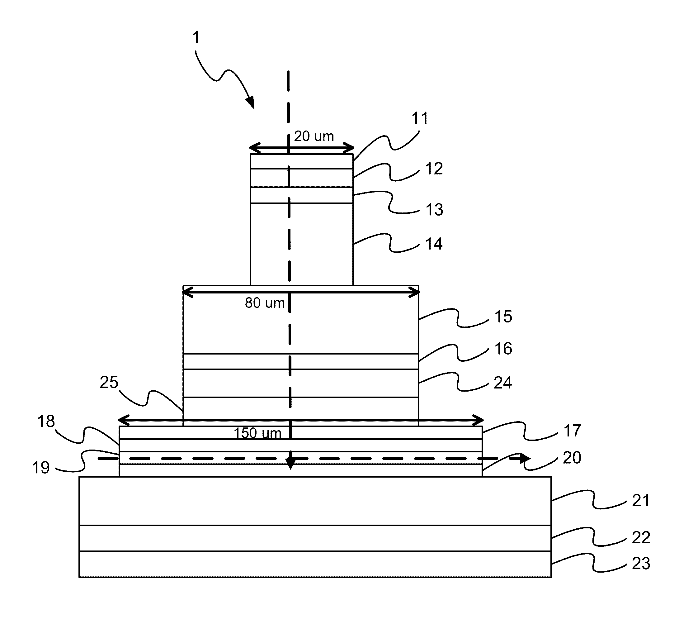
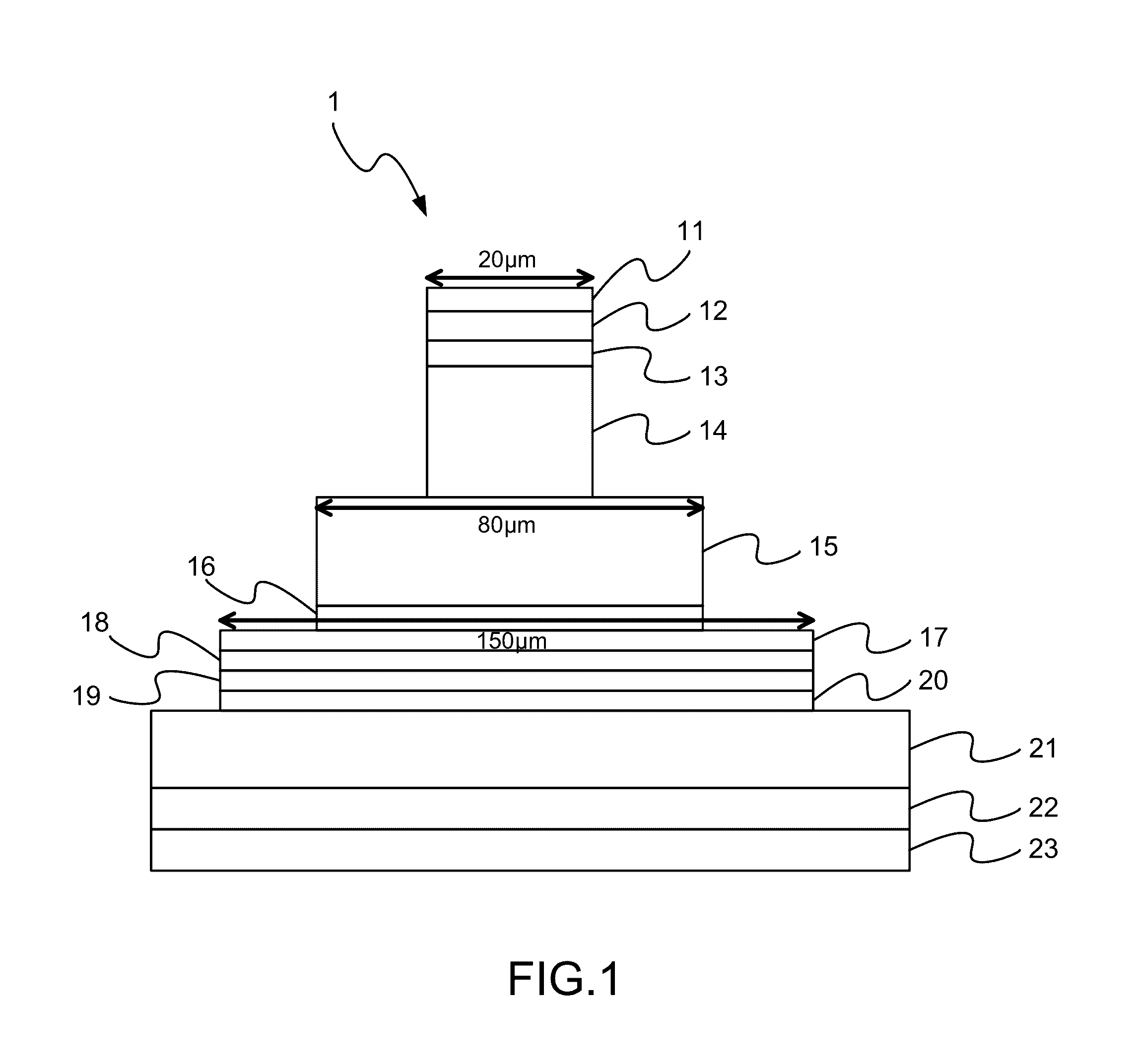
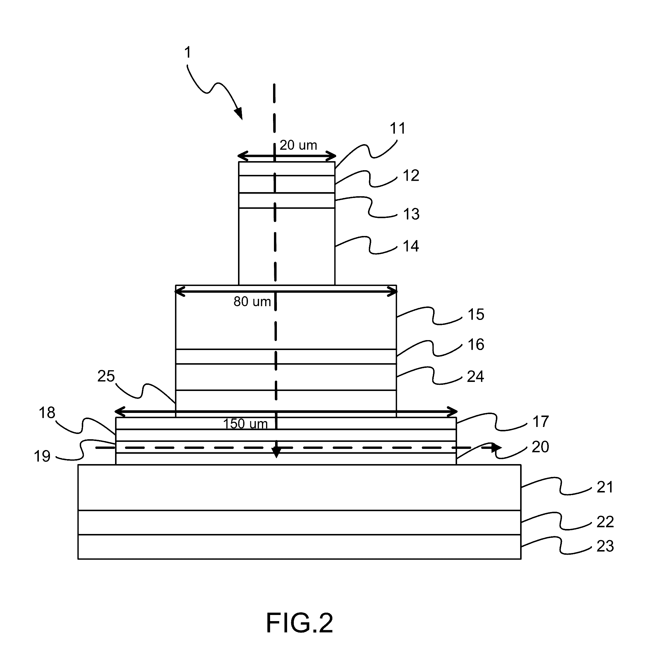
[0018]Please refer to FIG. 1-FIG. 4, which are sectional views showing a first and a second preferred embodiments according to the present invention; and views showing a one-dimensional and a two-dimensional field distributions under breakdown operation. As shown in the figures, the present invention is a photodetecting device having field confined by mesas (Avalanche Photodiode, APD), which, from top to bottom, comprises a p-type ohmic contact layer 11, a window layer 12, a first graded bandgap layer 13, a first absorption layer 14, a second absorption layer 15, a second graded bandgap layer 16, a field buffer layer 17, a first p-type field control layer 18, a multiplication layer 19, an n-type contact layer 20 and an n-type ohmic contact layer 21. The present invention is a device of ‘n-side (M-layer) down’ epitaxial layers 1 having a firs...


PUM


Abstract

A novel photodetecting device having field confined by mesas is provided. The device is an avalanche photodiode (APD) of indium aluminum arsenide (InAlAs). The device has epitaxial layers with a multiplication layer at bottom as a cathode. Hence, the strongest electric field is confined inside the bottom of the device to avoid surface breakdown. Double mesa is used to confine the electric field of the multiplication layer. Furthermore, a composite multiplication layer with supper thin thickness and wide bandgap is used to reduce the tunneling dark current. Hence, the thickness of equivalent multiplication layer can be reduced to enhance sensitivity.

Description

TECHNICAL FIELD OF THE INVENTION[0001]The present invention relates to a photodetecting device; more particularly, relates to an avalanche photodiode (APD) having an M-layer at bottom of epitaxial layers as a cathode to confined strongest field of the multiplication layer inside the bottom to avoid surface breakdown, where double mesa is used to confine the field of the multiplication layer.DESCRIPTION OF THE RELATED ART(S)[0002]To meet the demand for the internet of things (IOT) of larger virtual system and big data, it has long been unable to take on the traditional copper wire transmission task (≧˜100 m). It is still bound only to the bottomless transmission bandwidth of fiber. In consideration of the market size, cost and expected technology development for different transmission distances, four transmission interface are worked out for 400 Gigabit Ethernet (GbE) for different distances, which are 100 meters (m), 500 m, 2 kilo-meters (km) and 10 km. Therein, 400 giga-bits per se...

Claims


Application Information

Patent Timeline
IPC IPC(8): H01L31/107H01L31/0224H01L31/0304
CPCH01L31/107H01L31/022408H01L31/03046H01L31/1075Y02E10/544
Inventor SHI, JIN-WEI
Owner NAT CENT UNIV
Why Eureka
Try Eureka