
Booster antenna and method for producing same

a technology of booster antenna and booster antenna, which is applied in the direction of resonant antenna, conductive pattern formation, instruments, etc., can solve the problems of difficult to further reduce production costs, metal foil may be stripped from the substrate, and the rfid tag having an antenna circuit formed by metal foil has poor flexibility, etc., to achieve excellent electrical characteristics and flexibility, and inexpensive mass production

Inactive Publication Date: 2017-01-03
DOWA ELECTRONICS MATERIALS CO LTD
View PDF13 Cites 1 Cited by
  • Summary
  • Abstract
  • Description
  • Claims
  • Application Information

AI Technical Summary

Benefits of technology

[0010]It is therefore an object of the present invention to eliminate the aforementioned conventional problems and to provide a booster antenna, which has excellent electrical characteristics and flexibility and which can be inexpensively mass-produced, and a method for producing the same.
[0015]According to the present invention, it is possible to produce a booster antenna which has excellent electrical characteristics and flexibility and which can be inexpensively mass-produced.

Problems solved by technology

However, since these methods are not suit for mass production due to the limitation of their productivity, it is difficult to further reduce the production costs.
For that reason, there is a problem in that an RFID tag having an antenna circuit formed by a metal foil has bad flexibility although it has good electrical characteristics.
In addition, although a metal foil having a thickness of about 10 to 50 μm is generally used for forming an antenna circuit for an RFID tag, if the metal foil is too thick, the characteristics of the metal foil approach those of a metal plate for deteriorating the adhesion thereof to a substrate, so that there is some possibility that the metal foil may be stripped from the substrate when the RFID tag is bent.
Moreover, since the percentage of the metal in the metal foil is high, when RFID tag is bent, stress concentrates on the bent surface thereof, so that cracks are easy to be generated on the bent surface thereof.
As a result, the electrical characteristics thereof are deteriorated, and the breaking thereof is caused, so that it does not function as an antenna for an RFID tag.
On the other hand, if the percentage of a metal is decreased by using a conductive film of the metal component and a resin component in place of the metal foil in order to improve the flexibility of the RFID tag, it is possible to generally improve the flexibility by stress relaxation, but the amount of the metal component is decreased for deteriorating the electrical characteristics thereof, so that it does not have sufficient characteristics as those of an antenna for an RFID tag.
However, the conductive ink containing the small amount of silver particles is used for forming the thin conductive film having the thickness of 0.1 to 0.5 μm, and the percentage of silver in the conductive film is a high percentage which is approximately 100%, so that there is a problem in that the flexibility of the tag is bad similar to that in the method for transferring a metal foil to a substrate and in the method for etching a metal foil.
In an RFID tag chip integrated with an antenna, there is a problem in that the communication range thereof is short, so that it is desired to increase the communication range thereof.

Method used


Image

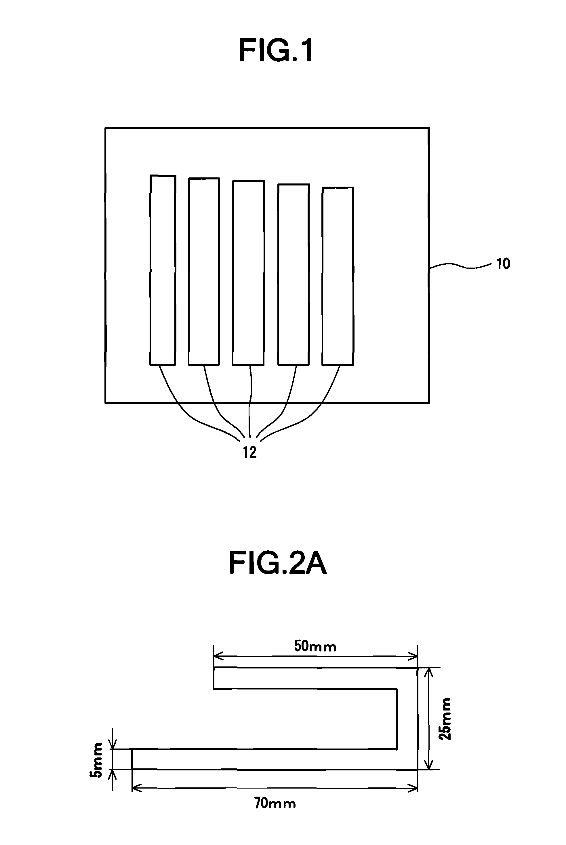
  • Booster antenna and method for producing same
  • Booster antenna and method for producing same
  • Booster antenna and method for producing same

Examples


examples 1-4

[0028]First, there was prepared an Ag ink (PFI-700 produced by PChem Associates Inc.) containing 60% by weight of Ag particles (silver particles having an average particle diameter of 10 nm), 3.0% by weight of polyvinyl chloride copolymer latex, 2.0% by weight of polyurethane thickener and 2.5% by weight of propylene glycol.

[0029]Then, a flexographic printing machine (multipurpose fine printing machine JEM Flex produced by Nihon Denshi Seiki Co., Ltd.) and a flexographic printing plate (produced by Watanabe Gosando Co., Ltd., Material of Printing Plate: Photosensitive Resin Plate AWP produced by Asahi Kasei Corporation, Grade DEF, Surface Processing 150 lines, 96 DOT %) were used for printing the above-described Ag ink on a substrate (PET (polyethylene terephthalate) film, Melinex (registered trademark) 545 produced by DuPont Teijin Films Limited) 10 at an anilox volume of 8 cc / m2 (400 lines / inch) and at a printing speed of 20 m / min. once (Example 1), twice (Example 2), three times ...

examples 8-10

Comparative Example 2

[0047]First, after the Ag ink used in Examples 1-4 was centrifuged at 3000 rpm for 10 minutes, the supernatant liquid was removed to prepare an Ag ink wherein the concentration of Ag particles was adjusted to be 70% by weight.

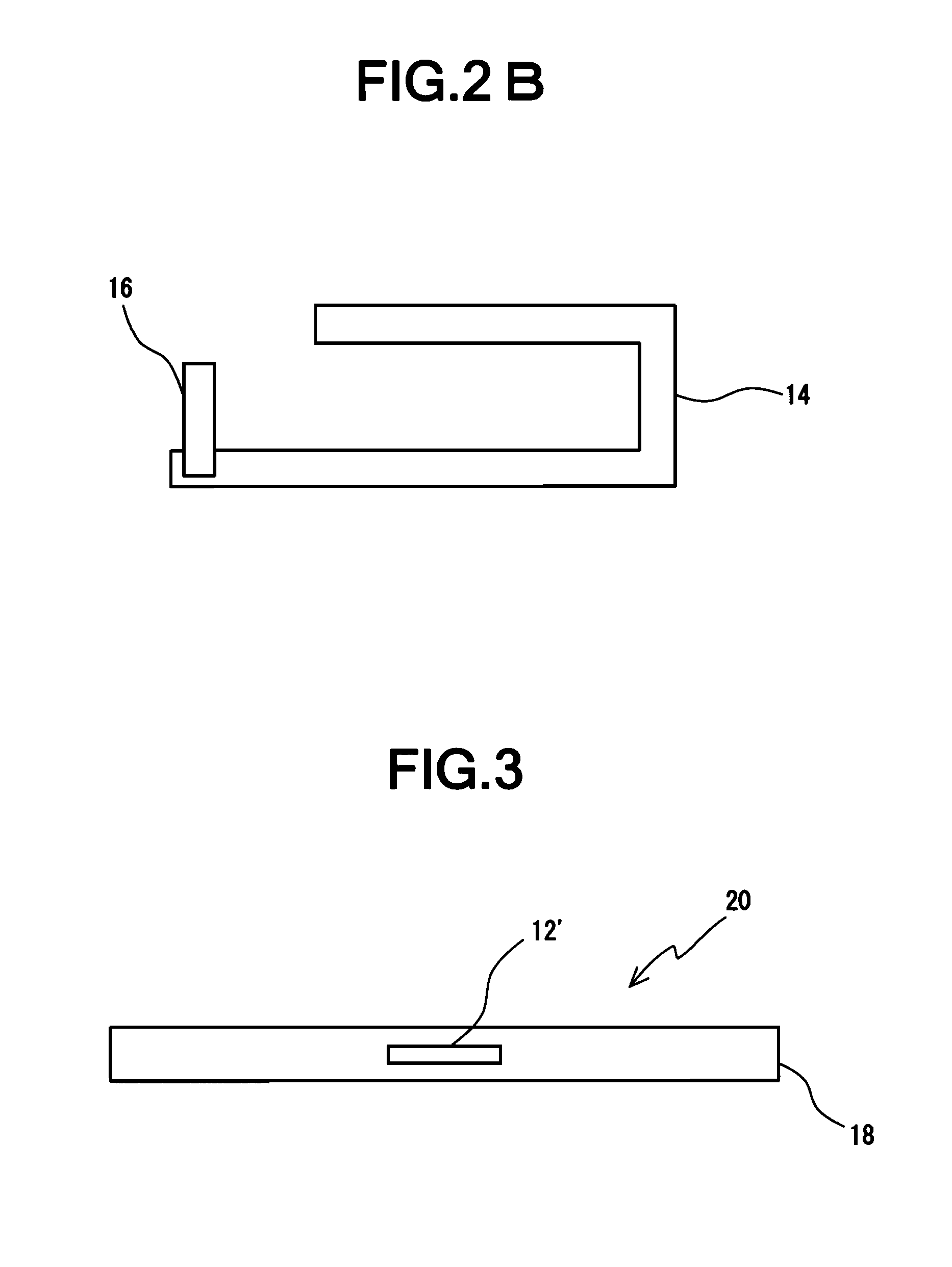
[0048]By the same method as that in Examples 1-4 except that the Ag ink thus prepared was used to be printed once (Example 8), twice (Example 9), three times (Example 10) and four times (Comparative Example 2), respectively, a conductive film was obtained, and then, an RFID tag chip-mounted booster antenna and a bending test sample were produced. Then, by the same method as that in Examples 1-4, the thickness, electrical resistance and surface resistivity of the conductive film were measured, and the volume resistivity of the conductive film and the percentage of Ag in the conductive film were calculated. Also, by the same method as that in Examples 1-4, the communication range of the RFID tag chip-mounted booster antenna was measured, and ...

examples 11-13

Comparative Examples 3-4

[0051]By the same method as that in Examples 1-4 except that the Ag ink was printed at an anilox volume of 20 cc / m2 (150 lines / inch) once (Example 11), twice (Example 12), three times (Example 13), four times (Comparative Example 3) and eight times (Comparative Example 4), respectively, a conductive film was obtained, and then, an RFID tag chip-mounted booster antenna and a bending test sample were produced. Then, by the same method as that in Examples 1-4, the thickness, electrical resistance and surface resistivity of the conductive film were measured, and the volume resistivity of the conductive film and the percentage of Ag in the conductive film were calculated. Also, by the same method as that in Examples 1-4, the communication range of the RFID tag chip-mounted booster antenna was measured, and the resistance deteriorated rate of the bending test sample was obtained.

[0052]As a result, the thickness of the conductive film was 2.2 μm (Example 11), 3.6 μm...


PUM

PropertyMeasurementUnit
volume resistivityaaaaaaaaaa
thicknessaaaaaaaaaa
particle diameteraaaaaaaaaa

Abstract

A silver particle dispersing solution, which contains 50-70% by weight of silver particles having an average particle diameter of 20 nm or less, is applied on a substrate by the flexographic printing, and then, calcined to produce a booster antenna wherein a silver conductive film, which contains 10-50% by volume of a sintered body of the silver particles and which has a volume resistivity of 3-100 μΩ·cm, a surface resistivity of 0.5Ω / □ or less and a thickness of 1-6 μm, is formed on the substrate. Thus, there is provided a booster antenna which has excellent electrical characteristics and flexibility and which can be inexpensively mass-produced.

Description

TECHNICAL FIELD[0001]The present invention relates generally to a booster antenna and a method for producing the same. More specifically, the present invention relates to a booster antenna for an RFEI tag and a method for producing the same.BACKGROUND ART[0002]RFID tags utilize the RFID (Radio Frequency Identification (Identification Technique based on Radio Communication)), and are thin, light and small electronic devices, each of which has a semiconductor chip for storing data, such as an identification number, and an antenna for transmitting and receiving radio waves.[0003]Such RFID tags are expected to be widely utilized in various service environments in various fields, such as physical distribution management, and are desired to be mass-produced to reduce the production costs thereof to be spread. Antennas for RFID tags are required to have a low electrical resistance in order to increase the data transmittable / receivable range (communication range) thereof to reduce data loss...

Claims


Application Information

Patent Timeline
Patent Type & Authority Patents(United States)
IPC IPC(8): H01Q1/38H01Q1/22H05K1/09G06K19/077H01Q1/36H01Q9/04H05K1/16H05K3/12
CPCH01Q1/364G06K19/07773G06K19/07794H01Q1/2225H01Q1/38H01Q9/0407H05K1/097H05K1/165H05K3/1275H05K2201/10098Y10T29/49016G06K19/07G06K19/077H01P11/00
Inventor ITOH, DAISUKEFUJITA, HIDEFUMIMURANO, YUKONNO, SHINICHI
Owner DOWA ELECTRONICS MATERIALS CO LTD
Learn More