Double-sided transparent conductive film and touch panel

a technology of transparent conductive film and touch panel, which is applied in the direction of instruments, non-metal conductors, non-insulated conductors, etc., can solve the problems of film breaking or scratching, affecting the adhesion of the transparent conductive layer 4, and reducing the productivity of the film, so as to improve the adhesion and reduce the glaringness. , the effect of improving the adhesion

Active Publication Date: 2017-03-28
NITTO DENKO CORP
View PDF41 Cites 3 Cited by
  • Summary
  • Abstract
  • Description
  • Claims
  • Application Information

AI Technical Summary

Benefits of technology

[0032]The anti-blocking layer 2a has, on a surface thereof, a flat portion 21 and protrusion portions 22. The formation of the protrusion portions 22 is caused by respective particles 5. In the double-sided transparent conductive film 10, the value obtained by subtracting the thickness TA of the flat portion 21 of the anti-blocking layer 2a from the mode diameter d of the particles 5 is larger than the thickness To of the optical adjusting layer 3a. When the optical adjusting layer 3a is formed by wet coating, the flat portion 21 of the anti-blocking layer 2a is buried by the optical adjusting layer 3a so that the height of the protrusion portion 22 is relatively decreased. Thus, the anti-blocking layer 2a may lose blocking resistance. The double-sided transparent conductive film 10 is formed in such a manner that the mode diameter d of the particles 5, the thickness TA of the flat portion 21 and the thickness To of the optical adjusting layer 3a satisfy the specific relationship. Thus, even when the optical adjusting layer 3a is formed by wet coating, the protrusion portions 22 of the anti-blocking layer 2a can be prevented from being lost. As a result, the protrusion portions 22 can cause the generation of protrusions also in the surface of the optical adjusting layer 3a, so that the double-sided transparent conductive film can exhibit good anti-blocking property. In FIG. 1, the particles 5 having the mode diameter d have been illustrated. However, the anti-blocking layer 2a may contain particles 5 having a particle diameter other than the mode diameter d as far as the advantageous effects of the present invention are not damaged.
[0033]In the double-sided transparent conductive film 10, usually, the thickness of the anti-blocking layer 2a is set into the order of micrometers while the thickness of each of the optical adjusting layer 3a and the transparent conductive layer 4a is set into the order of nanometers, which is a very small thickness. Thus, the transparent conductive layer 4a as the outermost surface layer follows the protrusions of the optical adjusting layer 3a to have protrusions. This is the same as in the lower surface side of the base material film 1 in FIG. 1.
[0034]The haze of the double-sided transparent conductive film is not particularly limited as far as the film can ensure required transparency. The haze is preferably 5% or less, more preferably 4% or less, even more preferably 3% or less. The lower limit of the haze is preferably 0%. In many cases, however, the haze is generally 0.3% or more by the presence of the protrusions in the outermost surface layers, and so on.<Base Material Film>
[0035]The base material film 1 is not particularly limited, and various kinds of plastic films having transparency are used. Examples of the material thereof include a polyester-based resin, an acetate-based resin, a polyether sulfone-based resin, a polycarbonate-based resin, a polyamide-based resin, a polyimide-based resin, a polyolefin-based resin, a polycycloolefin-based resin such as a polynorbonene-based resin, a (meth)acryl-based resin, a polyvinyl chloride-based resin, a polyvinylidene chloride-based resin, a polystyrene-based resin, a polyvinyl alcohol-based resin, a polyarylate-based resin and a polyphenylene sulfide-based resin. Among them preferable are a polycycloolefin-based resin, a polyester-based resin, a polycarbonate-based resin and a polyolefin-based resin. A polycycloolefin-based resin is especially preferable.
[0036]The thickness of the base material film 1 is preferably in a range of 2 to 200 μm, more preferably in a range of 20 to 180 μm. If the thickness of the base material film 1 is less than 2 μm, the mechanical strength of the base material film 1 may become insufficient, thus making it difficult to perform an operation to continuously form the optical adjusting layer 3 and the transparent conductive layer 4 with the film base material formed in a roll shape. On the other hand, if the thickness is more than 200 μm, the scratch resistance of the transparent conductive layer 4 and dotting property as intended for use in a touch panel may not be improved.
[0037]The surface of the base material film 1 may be subjected beforehand to an etching treatment or a undercoating treatment such as sputtering, plasma treatment, corona discharge, flame, ultraviolet-ray irradiation, electron-beam irradiation, chemical conversion or oxidation to improve adhesion with an anti-blocking layer, an optical adjusting layer and the like which are formed on the film base material. The surface of the film base may be freed from dust and cleaned by solvent cleaning or ultrasonic cleaning as necessary before the anti-blocking layer and the optical adjusting layer are formed.<Anti-Blocking Layer>

Problems solved by technology

However, in the roll-to-roll manner, films superimposed onto each other may adhere closely to each other and may become hard to be peeled from each other (the so-called blocking).
In some cases, the films may be broken or scratched to be declined in productivity.
However, when an optical adjusting layer is formed onto the anti-blocking layer through a wet coating process, the protrusion portions of the anti-blocking layer are lost by a liquid for the coating so that this layer does not exhibit anti-blocking property.

Method used


Image

  • Double-sided transparent conductive film and touch panel
  • Double-sided transparent conductive film and touch panel

Examples


example 1

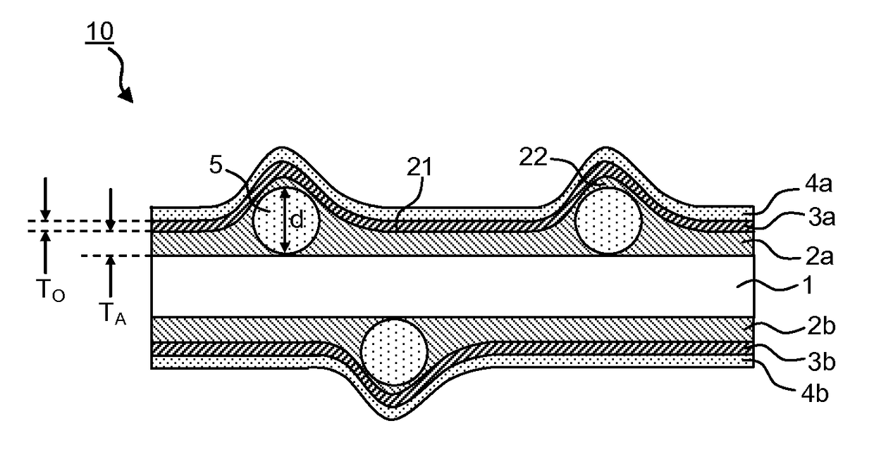
[0074]Prepared was a coating composition containing a plurality of mono-dispersible particles (manufactured by Soken Chemical Engineering Co., Ltd., trade name “SX-130H”) having a mode diameter of 1.3 μm, a binder resin (manufactured by DIC Corporation, trade name “UNIDIC RS29-120”), and ethyl acetate as a solvent. The addition amount of the particles was 0.2 parts based on 100 parts of the binder resin. Next, a gravure coater was used to apply the coating composition onto the both sides of a long base material film (manufactured by Nippon Zeon Co., Ltd., trade name “ZEONOA”) having a thickness of 100 μm in such a manner that the applied films would each have a thickness of 1.0 μm after dried. The workpiece was heated at 80° C. for 1 minute to dry the applied films. Thereafter, the workpiece was irradiated with ultraviolet rays giving a cumulative light quantity of 250 mJ / cm2 from a high-pressure mercury lamp to form anti-blocking layers.

[0075]Next, a gravure coater was used to appl...

example 2

[0078]A double-sided transparent conductive film was prepared in the same manner as in Example 1 except that monodisperse particles having a mode diameter of 1.5 μm (manufactured by SEKISUI PLASTICS CO., Ltd., trade name “XX-184AA”) were used as particles, and the added amount of the particles was 0.3 parts based on 100 parts of the binder resin.

example 3

[0079]A double-sided transparent conductive film was prepared in the same manner as in Example 1 except that monodisperse particles having a mode diameter of 1.9 μm (manufactured by Soken Chemical Engineering Co., Ltd., trade name “MX-180TA”) were used as particles, and the added amount of the particles was 0.2 parts based on 100 parts of the binder resin.


PUM

PropertyMeasurementUnit
thicknessaaaaaaaaaa
reflectanceaaaaaaaaaa
thicknessaaaaaaaaaa

Abstract

A double-sided transparent conductive film including a base material film, having an anti-blocking layer, an optical adjusting layer and a transparent conductive layer formed in this order on each of both sides of the base material film, wherein an anti-blocking layer containing particles is formed at least one of: a location between the base material film and one optical adjusting layer; and a location between the base material film and the other optical adjusting layer, the anti-blocking layer has a flat portion and protrusion portions caused by the particles, and a value obtained by subtracting a thickness of the flat portion of the anti-blocking layer from a mode diameter of the particles is larger than a thickness of the optical adjusting layer.

Description

BACKGROUND OF THE INVENTION[0001]Field of the Invention[0002]The present invention relates to a double-sided transparent conductive film, and a touch panel.[0003]Description of the Related Art[0004]In recent years, projected-capacitive touch panels or matrix-type resistive touch panels can attain multi-point input (multi-touch) to be excellent in operability. Demands therefor have been rapidly increasing. As an electrode member of such a touch panel, a double-sided transparent conductive film is suggested, in which transparent conductive thin films are formed on both sides of a transparent film base material, respectively.[0005]A touch panel as described above makes use of a double-sided transparent conductive film having patterned transparent conductive layers. As the material of the transparent conductive layers, indium / tin composite oxide (ITO) is widely used from the viewpoint of the visible ray transmittance thereof. However, the refractive index of ITO is high. Thus, when a tr...

Claims


Application Information

Patent Timeline
Patent Type & Authority Patents(United States)
IPC IPC(8): H01B5/14G06F3/041H01B1/08H05K1/02H01B5/00
CPCH01B5/002G06F3/0412H01B1/08H01B5/14H05K1/0274H05K1/0298G06F2203/04103Y10T428/24364G06F3/044G06F3/045G06F3/041
Inventor TAKADA, KATSUNORIHASHIMOTO, NAOKIHIRAOKA, SHINYAIKAI, KAZUHIROKURAMOTO, HIROKITAKAO, HIROYUKITSUNO, NAOKIUMEMOTO, TORU
Owner NITTO DENKO CORP
Why Eureka
Try Eureka