Method for producing a group III nitride semiconductor crystal and method for producing a GaN substrate

a technology of nitride and semiconductor crystal, which is applied in the direction of single crystal growth, chemistry apparatus and processes, from melt solutions, etc., can solve the problems of cracks and new dislocations, and achieve the effect of reducing dislocation density and dislocation density

Active Publication Date: 2017-06-27
TOYODA GOSEI CO LTD
View PDF48 Cites 0 Cited by
  • Summary
  • Abstract
  • Description
  • Claims
  • Application Information

AI Technical Summary

Benefits of technology

[0010]The present invention has been conceived in order to overcome the aforementioned drawbacks involved in conventional techniques. Thus, an object of the present invention is to provide a method for producing a Group III nitride semiconductor crystal and a method for producing a GaN substrate, where the propagation of dislocations and the occurrence of cracks can be certainly reduced on the growth substrate, and the Group III nitride semiconductor crystal can be easily separated from the seed crystal.
[0015]In the above method for producing a Group III nitride semiconductor crystal, a semiconductor crystal grows not on the unexposed portion which is covered with the mask layer, but on the exposed portion which is not covered with the mask layer semiconductor crystal. Here, “the mask layer” is a layer to inhibit the growth of the semiconductor crystal. Therefore, only dislocations on the exposed portion of the underlayer are inherited to the growing semiconductor crystal. Thus, some of the dislocations are not inherited from the underlayer, and a semiconductor crystal with a low dislocation density can be grown. The non-crystal portions are not connected with the grown semiconductor crystal or the underlayer because the non-crystal portions are liquid at the growth temperature. Therefore, a semiconductor crystal grows with the stress from the mask hardly applied, thereby minimizing the occurrence of the dislocations at the merged interface.
[0016]A second aspect of the present invention is a specific embodiment of the method for producing a Group III nitride semiconductor crystal of the first aspect, wherein the exposed portion comprises a plurality of growth starting regions discretely disposed and connecting portions to connect the growth starting regions. At this time, the dislocations at the connecting portions are not inherited to the growing semiconductor layer. Even if a distance between the growth starting regions is large, uniform lateral growth can be achieved, that is, dislocations can be effectively reduced.
[0032]On the thus produced Group III nitride semiconductor substrate, the transfer of dislocations is blocked by the mask, and dislocations hardly occur even at the joint interface. That is, the dislocations of the Group III nitride semiconductor substrate are sufficiently smaller than those of the conventional substrate. The area of the seed crystal that is in contact with the Group III nitride semiconductor crystal is sufficiently small. Therefore, the Group III nitride semiconductor crystal can be easily separated from the seed crystal.
[0037]The present invention enables provision of a method for producing a Group III nitride semiconductor crystal exhibiting no residual stresses or cracks and having a remarkably reduced dislocation density, and a method for producing a Group III nitride semiconductor substrate, e.g., GaN substrate, exhibiting no residual stresses or cracks and having a remarkably reduced dislocation density.

Problems solved by technology

However, in the method disclosed in Japanese Patent Application Laid-Open (kokai) No. 2005-12171, dislocations propagating on the mask layer can be reduced, but the stress from the mask layer is applied to the semiconductor crystal, resulting in two problems: (1) new dislocations occur at the joint interface of growing crystals, and (2) cracks occur.

Method used


Image

  • Method for producing a group III nitride semiconductor crystal and method for producing a GaN substrate
  • Method for producing a group III nitride semiconductor crystal and method for producing a GaN substrate
  • Method for producing a group III nitride semiconductor crystal and method for producing a GaN substrate

Examples


embodiment 1

[0054]Embodiment 1 will be described. In Embodiment 1, a Group III nitride semiconductor crystal is grown on a GaN self-standing substrate.

1. Group III Nitride Semiconductor Crystal

1-1. GaN Crystal

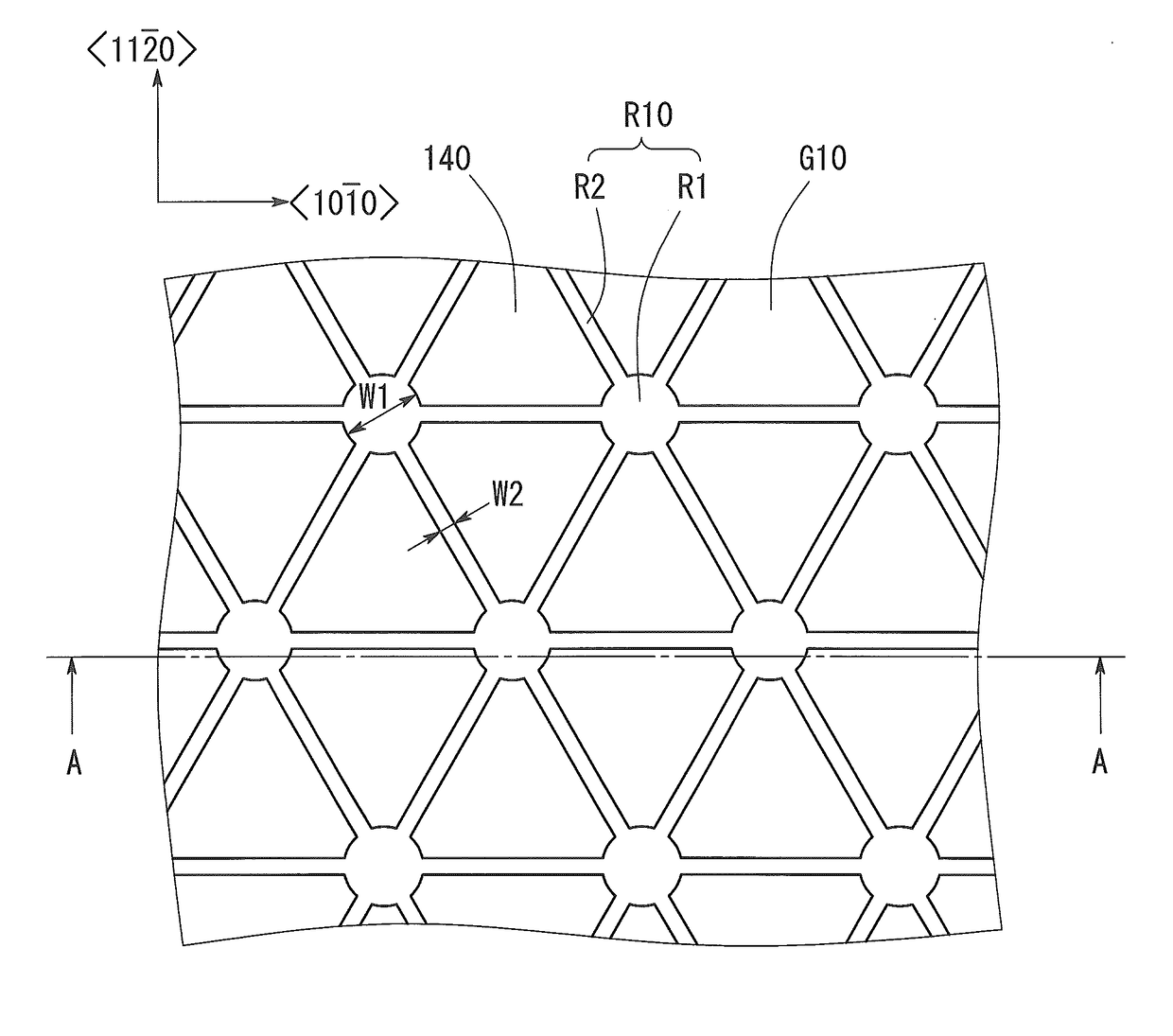
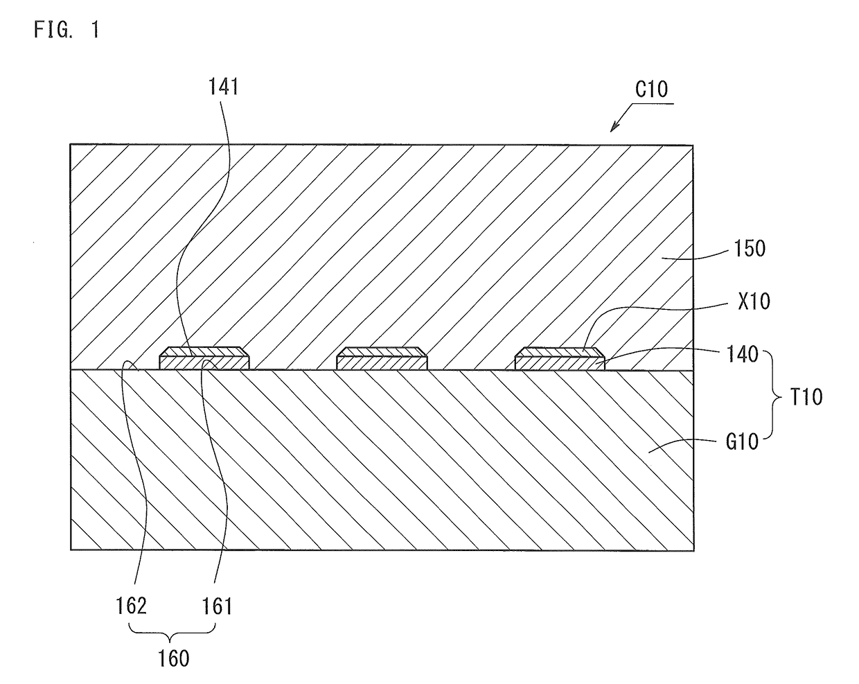
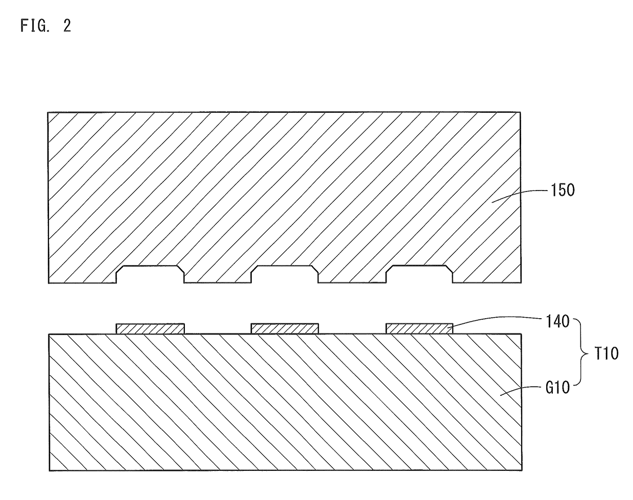
[0055]FIG. 1 shows the structure of GaN crystal C10 produced through the method for producing a Group III nitride semiconductor crystal according to Embodiment 1. The GaN crystal C10 of Embodiment 1 is produced through a flux method. The GaN crystal C10 has a seed crystal T10 and a GaN layer 150. The seed crystal T10 has a GaN substrate G10 and a patterned mask layer 140. Non-crystal portions X10, i.e., inclusions, molten mixture, gasses of nitrogen, etc., space, etc., are formed between the mask layer 140 of the seed crystal T10 and the GaN layer 150.

[0056]The mask layer 140 is formed on the GaN substrate G10 as an underlayer, more specifically, on a portion 161 of a main surface 160 of the GaN substrate G10. The mask layer 140 is a flux resistant layer. The mask layer 140 is formed of, f...

embodiment 2

[0092]Embodiment 2 will be described. In Embodiment 2, the same procedure as that of Embodiment 1 is repeated, except that the seed crystal T10 is a GaN layer epitaxially grown on a sapphire substrate. Thus, the same description in relation to Embodiment 1 will be omitted.

1. Group III Nitride Semiconductor Crystal

1-1. GaN Crystal

[0093]FIG. 7 shows the cross-sectional structure of GaN crystal C20 produced through the method for producing a Group III nitride semiconductor crystal according to Embodiment 2. The GaN crystal C20 has a seed crystal T20 and a GaN layer 250. Non-crystal portions X20 are formed between the seed crystal T20 and the GaN layer 250.

[0094]The seed crystal T20 has a sapphire substrate S20, a low-temperature buffer layer 220, a GaN layer 230, and a patterned mask layer 240. On portions 261 of the top surface 260 of the GaN layer 230, the mask layer 240 is formed, and on the remaining portion, i.e., exposed portion 262 of the top surface 260 of the GaN layer 230, th...

embodiment 3

[0111]Embodiment 3 will be described. In Embodiment 3, a GaN crystal C30 having two-stage, i.e., the first stage and the second stage, mask layer is produced as shown in FIGS. 10A and 10B. FIG. 10A is a cross section cut along the B-B line of the triangle pattern in the plan view of FIG. 10B.

1. Group III Nitride Semiconductor Crystal

[0112]The GaN crystal C30 has a GaN substrate G30, a first mask layer 320, a first GaN layer 330, a second mask layer 340, and a second GaN layer 350. First non-crystal portions X30 are formed between the first mask layer 320 and the first GaN layer 330. Second non-crystal portions X40 are formed between the second mask layer 340 and the second GaN layer 350. As shown in FIGS. 10A and 10B, the second mask layer 340 is formed on an extension line perpendicular to the main surface of the GaN substrate G30 as viewed from the first exposed portion 361 (the first region R1 of the first stage) as a growth starting point of the first GaN layer 330. Moreover, a ...


PUM

PropertyMeasurementUnit
angleaaaaaaaaaa
pressureaaaaaaaaaa
thicknessaaaaaaaaaa

Abstract

The present invention provides a method for producing a Group III nitride semiconductor crystal and a GaN substrate, in which the transfer of dislocation density or the occurrence of cracks can be certainly reduced on a growth substrate, and the Group III nitride semiconductor crystal can be easily separated from a seed crystal. A mask layer is formed on a GaN substrate, to thereby form an exposed portion of the GaN substrate, and an unexposed portion of the GaN substrate. Through a flux method, a GaN layer is formed on the exposed portions of the GaN substrate in a molten mixture containing at least Group III metal and Na. At that time, non-crystal portions containing the components of the molten mixture are formed on the mask layer so as to be covered with the GaN layer grown on the GaN substrate and the mask layer.

Description

BACKGROUND OF THE INVENTION[0001]Field of the Invention[0002]The present invention relates to a method for producing a Group III nitride semiconductor crystal and to a method for producing a GaN substrate. More particularly, the invention relates to a method for producing a Group III nitride semiconductor crystal and to a method for producing a GaN substrate, which methods employ a flux method.[0003]Background Art[0004]A variety of methods for producing a semiconductor crystal are known, and examples thereof include vapor phase growth methods such as metalorganic chemical vapor deposition (MOCVD) and hydride vapor phase epitaxy (HVPE), molecular beam epitaxy (MBE), and liquid phase epitaxy (LPE). One technique of LPE is a flux method employing a Na flux.[0005]In the flux method, a molten mixture of metallic Na (sodium) and metallic Ga (gallium) is reacted with nitrogen under pressure for the growth of a GaN crystal. This method is expected to produce an inexpensive and high-quality ...

Claims


Application Information

Patent Timeline
Patent Type & Authority Patents(United States)
IPC IPC(8): C30B9/10H01L21/02H01L21/78
CPCH01L21/02647H01L21/0254H01L21/02623H01L21/02642H01L21/7806
Inventor KUMEGAWA, SHOHEIYAKUSHI, YASUHIDENAGAI, SEIJIMORIYAMA, MIKI
Owner TOYODA GOSEI CO LTD
Why Eureka
Try Eureka