Semiconductor structure and method for manufacturing the same

a technology of semiconductors and semiconductors, applied in the direction of semiconductor devices, basic electric elements, electrical appliances, etc., can solve the problems of gate threshold voltage reduction, signal-to-noise ratio (snr), and increase in power consumption, so as to suppress the short channel effect, reduce the steepness of the source/drain region, and improve the stress

Inactive Publication Date: 2017-06-27
INST OF MICROELECTRONICS CHINESE ACAD OF SCI
View PDF9 Cites 4 Cited by
  • Summary
  • Abstract
  • Description
  • Claims
  • Application Information

AI Technical Summary

Benefits of technology

[0008]In order to solve the above problems, the present invention provides a semiconductor structure and its manufacturing method, which are advantageous in providing the channel with good stress effect and increasing the steepness of the source / drain region, thereby suppressing the short channel effect.
[0026]Compared with the prior art, the technical solutions provided by the present invention have the following advantages: since a cavity is formed below the channel, the stress of the stress material source / drain region on both sides of the channel can act on the channel more concentratedly, thereby effectively enhancing the impact of stress on the channel carrier mobility and enhancing control on the channel performance; furthermore, the presence of the cavity below the channel is also beneficial to enhance the steepness of the source / drain region, thereby suppressing the short channel effect and improving the performance of the semiconductor devices.

Problems solved by technology

However, the reduction of the size of the MOS transistor results in the emergence of two well-known parasitic effects, i.e., short channel effect emerging as a result of reduction of the gate length and drain induced barrier lowering effect, which may deteriorate electrical properties of devices, such as reduction of gate threshold voltage, increase in power consumption, and signal-to-noise ratio (SNR) decline.
In order to control the short channel effect, more impurity elements such as phosphorus, boron and the like have to be doped in the channel, but which may easily lead to reduction of mobility of carries in the device channel.
Moreover, the distribution used to dope dopants into the channel can hardly control the problem of steepness, which may easily result in severe short channel effects; the thickness of gate oxides will also encounter a bottleneck of development, the thinning rate in the gate oxide thickness can hardly keep up with the reducing of the gate width, and gate dielectric leakage is increasing; and critical dimensions continue to shrink, which may easily cause the resistance of the source / region to increase continuously and the power consumption of the device to become greater.
However, the traditional silicon germanium strained silicon technology also begins to face bottlenecks, which can hardly provide stronger strain to the channel and cannot effectively enhance the performance of the semiconductor device.

Method used


Image

  • Semiconductor structure and method for manufacturing the same
  • Semiconductor structure and method for manufacturing the same
  • Semiconductor structure and method for manufacturing the same

Examples


Embodiment Construction

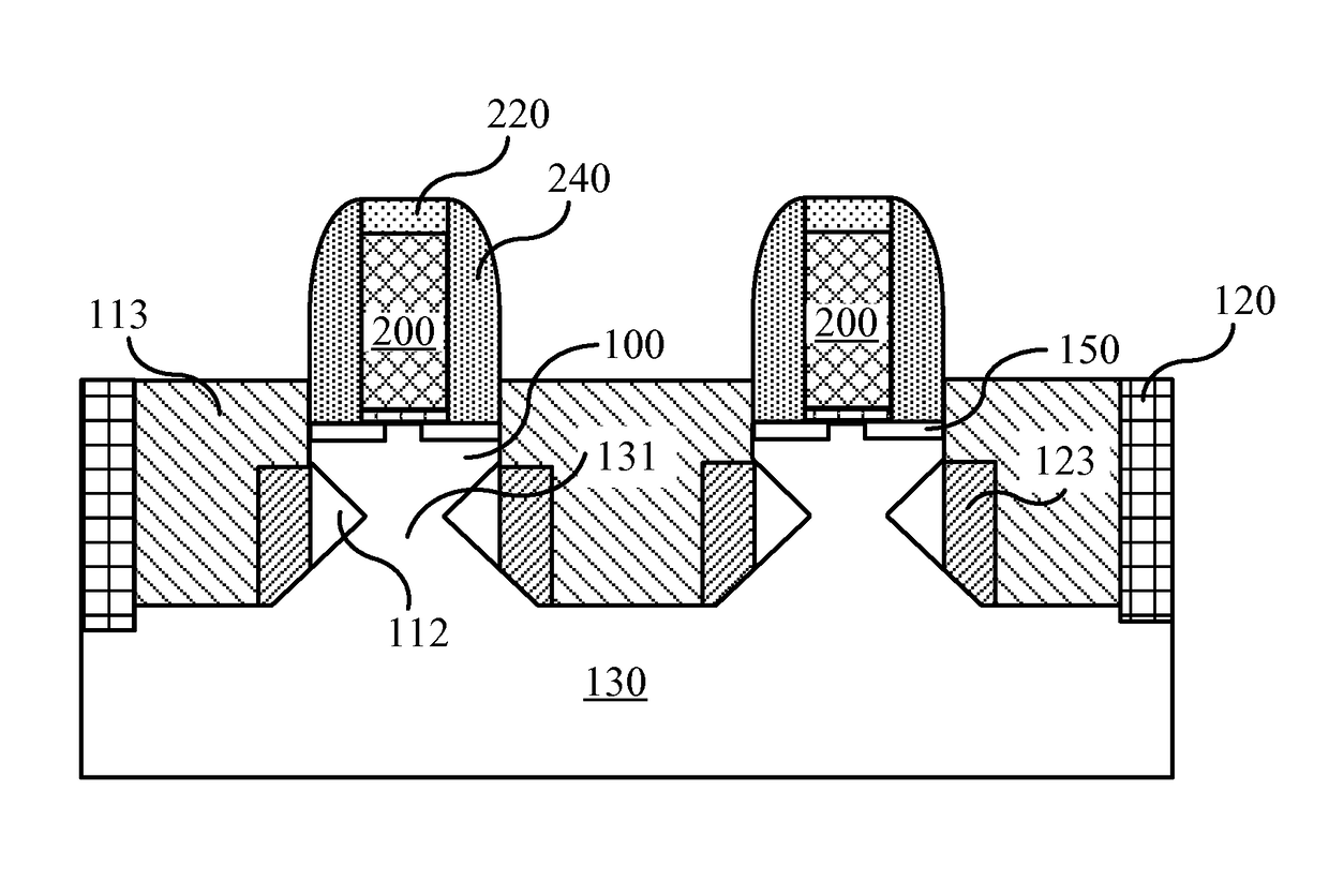
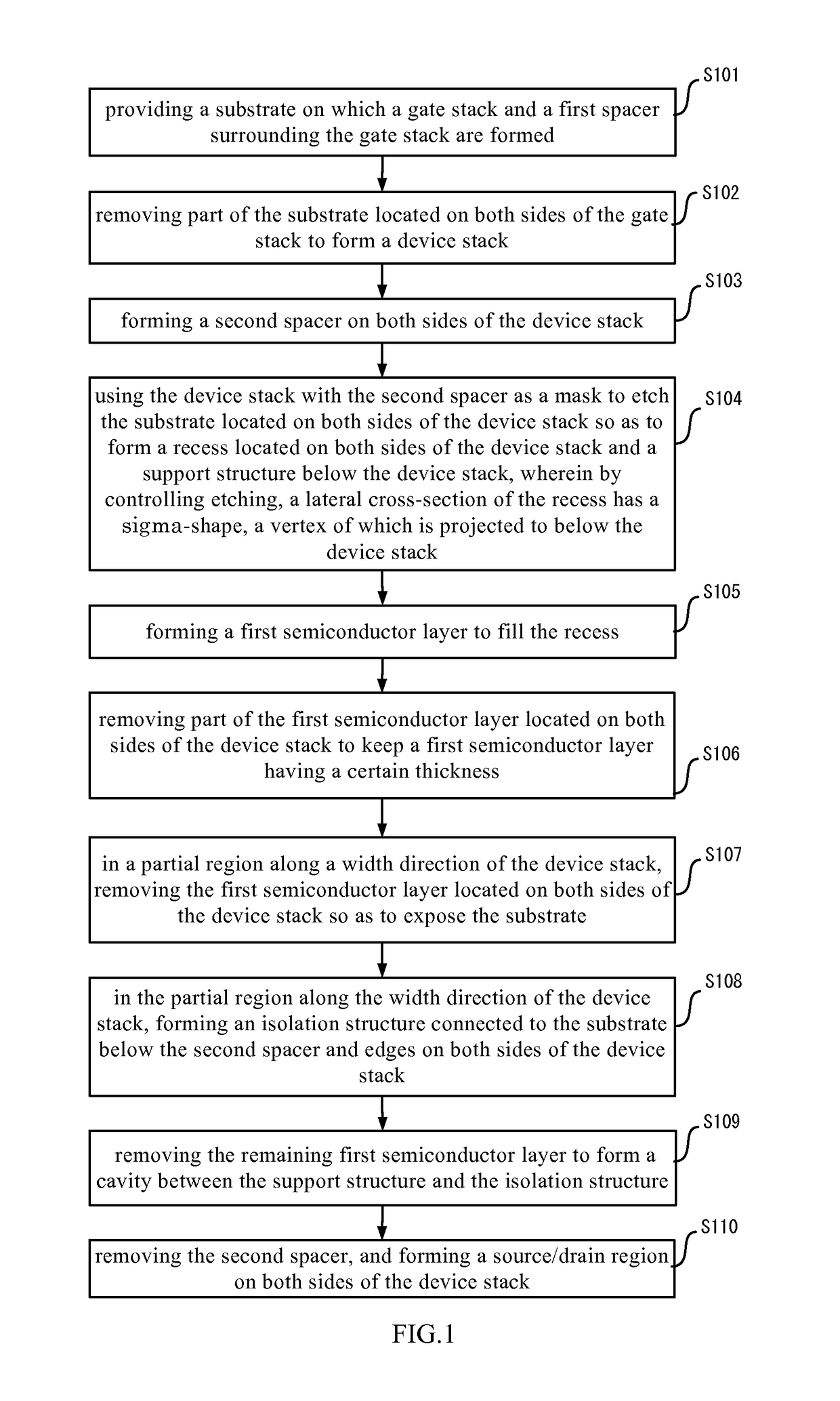
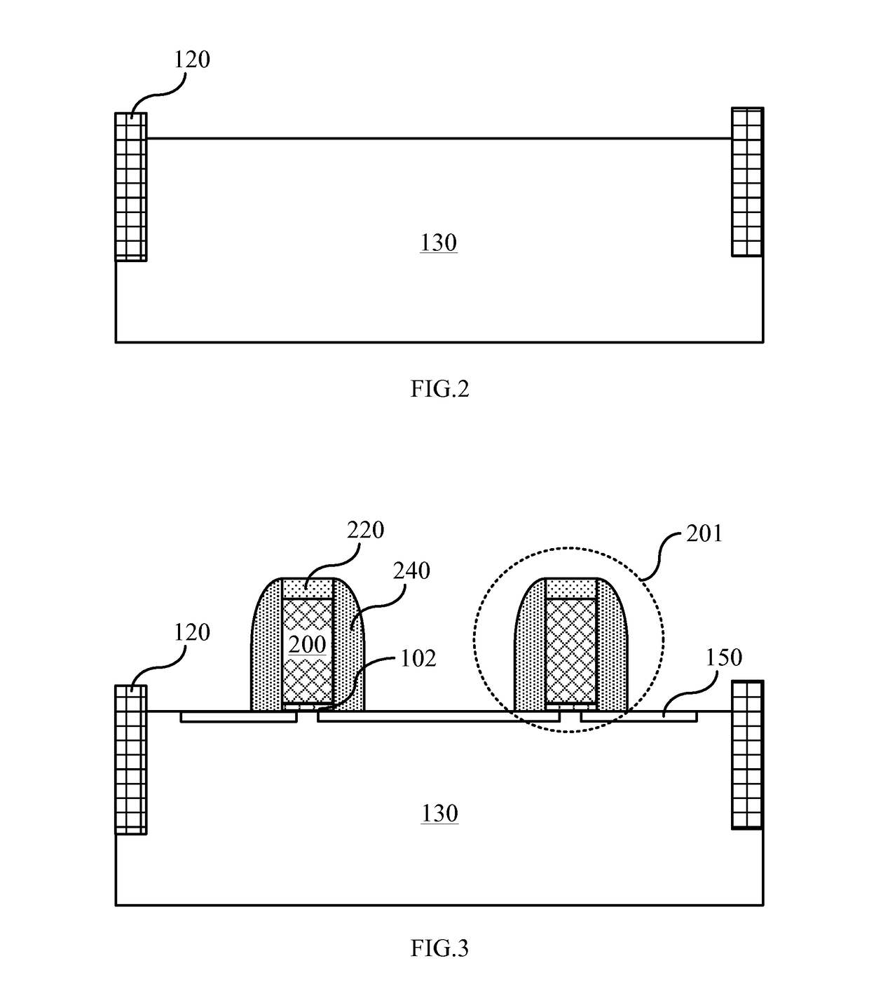
[0048]The embodiments of the present invention are described in detail below.

[0049]Illustrative examples of the embodiments are shown in the figures, and the same or similar reference numbers denote the same or similar components or components having the same or similar functions. The examples described with reference to the figures below are exemplary for explaining the present invention only, and cannot be construed as limiting the present invention. The following disclosure provides many different embodiments or examples to achieve different structures of the present invention. In order to simplify the disclosure of the present invention, members of specific examples and settings thereof will be described hereinafter. Of course, they are merely exemplary, and are not intended to limit the present invention. In addition, numbers and / or letters in the present invention can be repeated in different examples. Such repetition is for the purpose of simplification and clarity, which its...


PUM


Abstract

A semiconductor structure is provided, comprising a substrate (130), a support structure (131), a base region (100), a gate stack, a spacer (240), and a source / drain region, wherein the gate stack is located above the base region (100), and the base region (100) is supported above the substrate (130) by the support structure (131), wherein the support structure (131) has a sigma-shaped lateral cross-section; an isolation structure (123) is formed below edges on both sides of the base region (100), wherein a portion of the isolation structure (123) is connected to the substrate (130); a cavity (112) is formed between the isolation structure (123) and the support structure (131); and a source / drain region is formed on both sides of the base region (100) and the isolation structure (123). Accordingly, a method for manufacturing the semiconductor structure is also provided.

Description

CROSS REFERENCE TO RELATED APPLICATION[0001]This application is a national stage application, filed under 35 U.S.C. §371, of PCT Application No. PCT / CN2012 / 085359, filed on Nov. 27, 2012, entitled “SEMINCONDUCTOR STRUCTURE AND METHOD FOR MANUFACTURING THE SAME”, which claimed priority to Chinese Application No. 201210432008.6, filed on Nov. 2, 2012, all of which are hereby incorporated by reference in their entirety.[0002]The present application claims priority benefit of Chinese patent application No. 201210432008.6, filed on 2 Nov. 2012, entitled “SEMICONDUCTOR STRUCTURE AND METHOD FOR MANUFACTURING THE SAME”, which is herein incorporated by reference in its entirety.TECHNICAL FIELD[0003]The present invention relates to the field of semiconductor technology. In particular, the present invention relates to a semiconductor structure and a method for manufacturing the same.BACKGROUND ART[0004]Industrial demand requires IC circuits to have a higher density and reduced size of MOS tran...

Claims


Application Information

Patent Timeline
Patent Type & Authority Patents(United States)
IPC IPC(8): H01L21/336H01L29/417H01L29/165H01L29/161H01L29/16H01L21/762H01L21/308H01L21/027H01L21/02H01L29/08H01L21/8238H01L29/66H01L29/06H01L21/8234H01L29/78
CPCH01L29/7848H01L21/0243H01L21/0274H01L21/02381H01L21/02433H01L21/02529H01L21/02532H01L21/02639H01L21/308H01L21/76224H01L21/823412H01L21/823425H01L21/823468H01L21/823807H01L21/823814H01L21/823864H01L29/0653H01L29/0688H01L29/0847H01L29/161H01L29/165H01L29/1608H01L29/41783H01L29/6653H01L29/6656H01L29/66636H01L29/7834
Inventor ZHU, HUILONGYIN, HAIZHOULUO, ZHIJIONG
Owner INST OF MICROELECTRONICS CHINESE ACAD OF SCI
Why Eureka
Try Eureka