

Thin film transistor and fabrication method thereof, array substrate, and display device
a thin film transistor and substrate technology, applied in the field of display technology, can solve the problems of sub>off/sub>, low switching performance of tft, and low resistance, and achieve the effects of preventing effective corrosion, improving the switching performance of tft, and effectively simplifying fabrication
- Summary
- Abstract
- Description
- Claims
- Application Information
AI Technical Summary
Benefits of technology
Problems solved by technology
Method used
Image

Examples
first embodiment
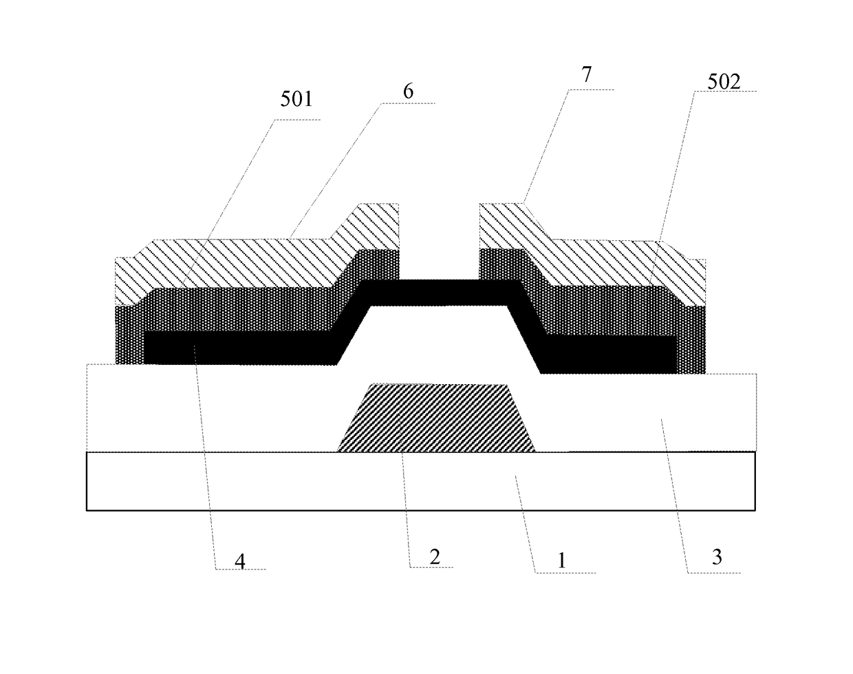
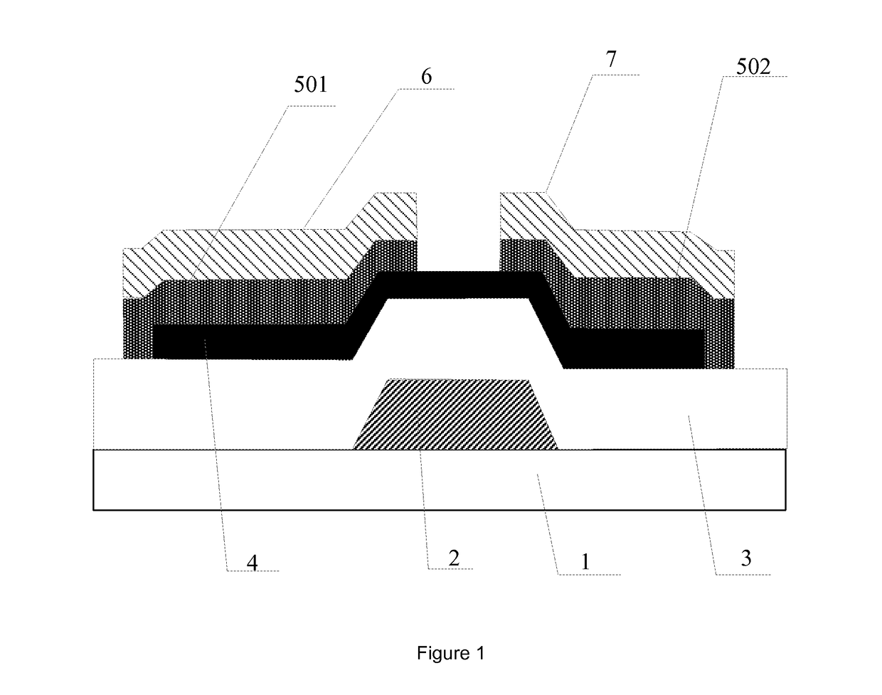
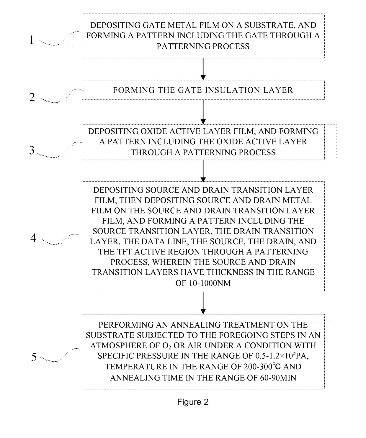
[0107]FIG. 1 is a cross-sectional diagram of a TFT according to the present invention, which illustrates a structure of a TFT. The TFT of this embodiment mainly includes a gate 2, a gate insulation layer 3, an oxide active layer 4, a source 6 and a drain 7 formed on a substrate 1. The TFT further includes a source and drain transition layer, the source and drain transition layer is formed between the oxide active layer 4 and the source 6, the drain 7, wherein parts of the source and drain transition layer corresponding to the source 6 and the drain 7 are a source transition layer 501 and a drain transition layer 502, respectively, and the source transition layer 501 and the drain transition layer 502 are separated from each other. Specifically, the source transition layer 501 may have the same pattern as the source 6, and the drain transition layer 502 may have the same pattern as the drain 7; alternatively, the source transition layer 501 and the drain transition layer 502 may resp...
second embodiment
[0122]FIG. 3 is a plan view of an array substrate according to the present invention, which illustrates a structure of one pixel unit, and FIG. 4 is a cross-sectional diagram viewed along line A0-A0 in FIG. 3. As illustrated in FIGS. 3 and 4, major structure of a common TFT array substrate in this embodiment mainly includes a gate line 11 formed on a substrate 1, a data line 12, a common electrode line 13, a pixel electrode 9 and a TFT formed on a substrate 1, the gate line 11 and the data line 12 which are perpendicular to each other and intersect define a pixel unit, the TFT and the pixel electrode 9 are formed within the pixel unit, the gate line 11 is used to provide a turned-on or cut-off voltage to the TFT, the TFT is used to control the data line 12 to provide a data voltage to the pixel electrode 9, and the common electrode line 13 is used to form a storage capacitor with the pixel electrode 13. The TFT further includes a source and drain transition layer, the source and dra...
third embodiment
[0139]This embodiment is a preferable embodiment of the present invention, FIG. 6 is a plan view of an array substrate according to the present invention, which illustrates a structure of one pixel unit, and FIG. 7 is a cross-sectional diagram viewed along line A1-A1 in FIG. 6. As illustrated in FIGS. 6 and 7, major structure of an active matrix / organic light emitting diode (AMOLED) array substrate in this embodiment mainly includes a gate line 11, a data line 12 and a power line 14, the data line 12 and the power line 14 are perpendicular to the gate lines 11, and define a pixel region together with two adjacent gate lines 11, in the pixel region, a first TFT (also referred to as a switching TFT) as an addressing element, a second TFT (also referred to as a driving TFT) for controlling an organic light emitting diode, a first pixel electrode 109 and a second pixel electrode 209 are formed, the first TFT is positioned at an intersection of the gate lines 11 and the data line 12, and...
PUM
 Abstract
Description
Claims
Application Information