Hybridization fin reveal for uniform fin reveal depth across different fin pitches

a technology of hybridization and fin reveal, applied in the field of hybridization fin reveal, can solve problems such as difficulty, and achieve the effect of uniform heigh

Inactive Publication Date: 2017-09-05
ELPIS TECH INC
View PDF16 Cites 14 Cited by
  • Summary
  • Abstract
  • Description
  • Claims
  • Application Information

AI Technical Summary

Benefits of technology

[0006]Another method for uniform fin reveal depth for semiconductor devices includes forming a liner over semiconductor fins and a substrate; forming one or more dielectric materials over the liner; dry etching the one or more dielectric materials to reveal semiconductor fins by a quasi-atomic layer etching (quasi-ALE) process to achieve depth uniformity across different fin pitches and different material types or qualities; isotropically etching the one or more dielectric materials with a plasma free reactive cleaning or remote plasma etch to compensate for lateral bias induced by the quasi-ALE process; deglazing the one or more dielectric materials to remove footings at the base of the fins to achieve the depth uniformity across different fin pitches and material types or qualities; and recessing the liner to a surface of the one or more dielectric materials.
[0007]A semiconductor device having a uniform height across different fin densities includes a semiconductor substrate having fins etched therein and including dense fin regions and isolation regions without fins. One or more dielectric layers are formed at a base of the fins and the isolation regions and have a uniform height across the fins and the isolation regions. The uniform height includes a less than 2 nanometer difference across the one or more dielectric layers.

Problems solved by technology

This is very difficult to do especially given the small process window for the two etch processes for the fin reveal, which is not comparable with multi-fin pitch CMOS (complementary metal oxide semiconductor) patterning.

Method used


Image

  • Hybridization fin reveal for uniform fin reveal depth across different fin pitches
  • Hybridization fin reveal for uniform fin reveal depth across different fin pitches
  • Hybridization fin reveal for uniform fin reveal depth across different fin pitches

Examples


Embodiment Construction

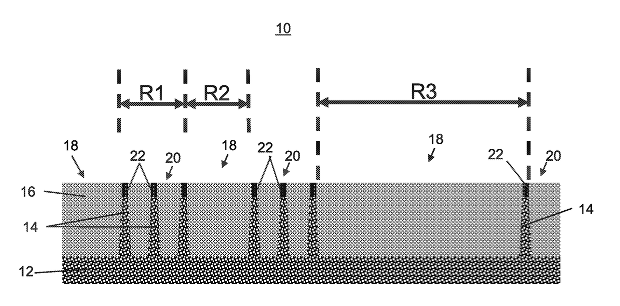
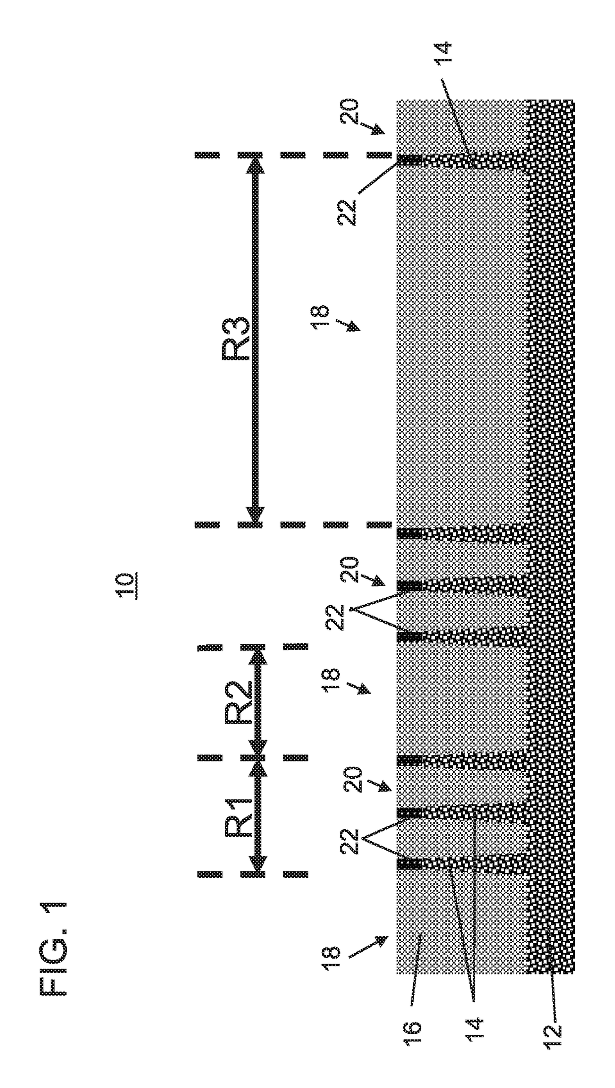
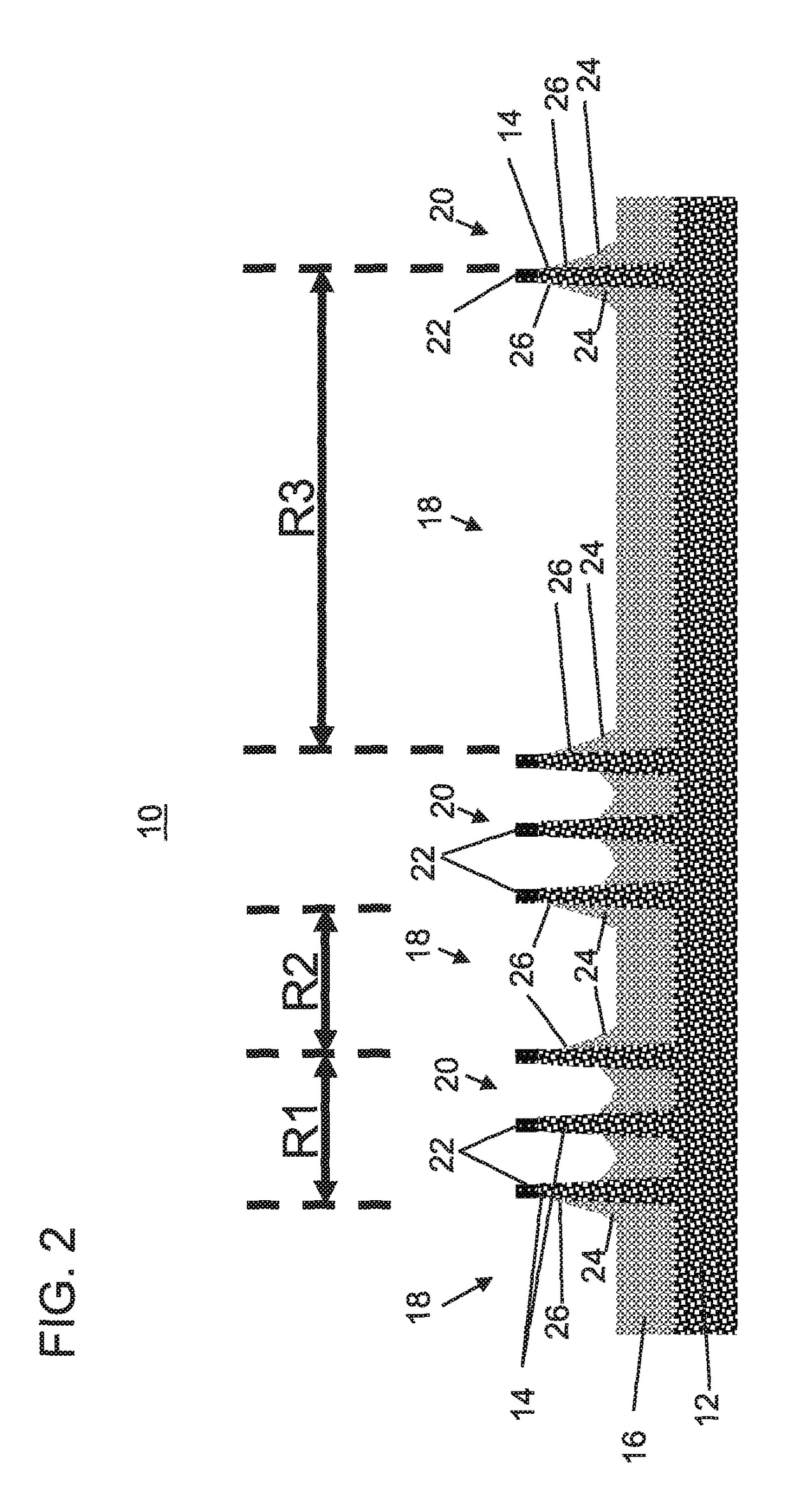
[0020]Embodiments of the present invention provide a hybrid fin reveal method to minimize differences in both vertical and lateral directions for shallow trench isolation material formed about the fins. The hybrid fin reveal provides uniformity across different fin densities and different dielectric quality films. In useful embodiments, a dry fin reveal process is employed such as, e.g., atomic layer etching (ALE), to achieve depth uniformity across different fin pitches. A plasma free reactive clean or remote plasma etch (downstream plasma etch) can then be employed to compensate for a lateral bias induced by the ALE process. An optional deglaze process can be employed to clean up remnants at a footing of the fins.

[0021]In other embodiments, fins can be formed with different pattern density regions (e.g., >2 regions), which include a hard mask (e.g., SiN) patterned on top of the fins. A protective etch selective liner can be deposited over the fins in some embodiments. Each region ...


PUM

PropertyMeasurementUnit
heightaaaaaaaaaa
depthaaaaaaaaaa
densityaaaaaaaaaa

Abstract

A method for uniform fin reveal depth for semiconductor devices includes dry etching a dielectric material to reveal semiconductor fins by a quasi-atomic layer etching (quasi-ALE) process to achieve depth uniformity across different fin pitches. A lateral bias induced by the quasi-ALE process is compensated for by isotropically etching the dielectric material.

Description

BACKGROUND[0001]Technical Field[0002]The present invention generally relates to semiconductor processing, and more particularly to methods and structures for fin reveals that preserve shallow trench isolation height (e.g., uniform fin reveal depth) regardless of fin density.[0003]Description of the Related Art[0004]Fin reveal processes typically employ a buffered HF etch process (wet etch) and an oxide removal etch (oxide etch) to reveal fins through an oxide layer during fin field effect transistor manufacturing. The wet etch process etches dense fin region regions (dense regions) at a faster etch rate while the oxide removal etch process etches isolation regions (iso regions) at a faster etch rate. The wet etch process does most of the material removal during the fin reveal, and the oxide removal process tunes the iso region fin reveal depth to attempt to match the fin reveal depth in the dense region. The etch rate of wet etch (e.g., HF) is very sensitive to oxide material qualit...

Claims


Application Information

Patent Timeline
Patent Type & Authority Patents(United States)
IPC IPC(8): H01L21/31H01L21/76H01L29/66H01L29/06H01L21/762H01L21/311H01L29/78
CPCH01L21/31116H01L21/76224H01L29/66795H01L29/0653H01L29/7851H01L21/823481H01L21/0206H01L21/31111H01L21/31138H01L21/76229H01L21/823431H01L29/0649
Inventor BI, ZHENXINGCANAPERI, DONALD F.DEVARAJAN, THAMARAI S.KANAKASABAPATHY, SIVANANDA K.LIE, FEE LIXU, PENG
Owner ELPIS TECH INC
Why Eureka
Try Eureka