Display device having MEMS transmissive light valve and method for forming the same

a technology of transmissive light valve and display device, which is applied in the direction of optical elements, coatings, instruments, etc., can solve the problems of low light utilization rate, small view angle range, complex structure, etc., to improve the performance and reliability of the circuit, improve the performance of the driving circuit and alignment accuracy, and reduce leakage current

Active Publication Date: 2017-09-26
INTELLECT CHIP ELECTRONIC TECH CO LTD
View PDF41 Cites 0 Cited by
  • Summary
  • Abstract
  • Description
  • Claims
  • Application Information

AI Technical Summary

Benefits of technology

[0020]Forming the driving circuit and the MEMS transmissive light valve on the SOI substrate can effectively reduce leakage current, and improve performance and reliability of the circuit.
[0021]In addition, the method of the present disclosure can improve performance of the driving circuit and alignment accuracy between sensing units, simplify manufacturing process, optimize device performance, shorten manufacturing cycle, decrease device size, and reduce manufacturing cost.

Problems solved by technology

The conventional liquid crystal display devices have disadvantages of low light utilization rate, small view-angle range, complex structure, and high cost.
However, the driving circuit of the conventional display device needs to be formed in another chip, which may result in a big size of the display device.
Besides, the manufacturing process of the display panel is not compatible with semiconductor manufacturing process, which means the display panel and the driving circuit cannot be manufactured in a same process, resulting in poor compatibility of the display device.

Method used


Image

  • Display device having MEMS transmissive light valve and method for forming the same
  • Display device having MEMS transmissive light valve and method for forming the same
  • Display device having MEMS transmissive light valve and method for forming the same

Examples


Embodiment Construction

[0025]In order to clarify the objects of the disclosure, the embodiments of the present disclosure will be described in detail in conjunction with the accompanying drawings.

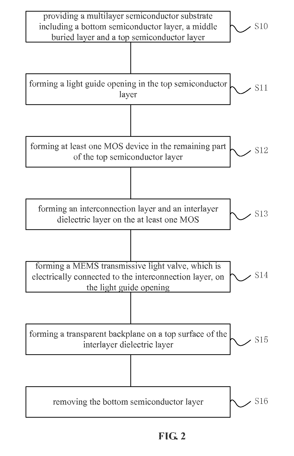
[0026]A method for forming a display device having a MEMS transmissive valve is provided in embodiments of the present disclosure. FIG. 2 illustrates a schematic flow chart of a method for forming a display device having a MEMS transmissive valve according to one embodiment of the present disclosure. As shown in FIG. 2, the method includes:

[0027]S10, providing a multilayer semiconductor substrate including a bottom semiconductor layer, a middle buried layer and a top semiconductor layer;

[0028]S11, forming a light guide opening in the top semiconductor layer;

[0029]S12, forming at least one MOS device in the remaining part of the top semiconductor layer;

[0030]S13, forming an interconnection layer and an interlayer dielectric layer on the at least one MOS;

[0031]S14, forming a MEMS transmissive light valve, which is ...


PUM

PropertyMeasurementUnit
thickaaaaaaaaaa
thickaaaaaaaaaa
thicknessaaaaaaaaaa

Abstract

A display device having a MEMS transmissive light valve and a method for forming the same are provided. The method includes: providing a multilayer semiconductor substrate comprising a bottom semiconductor layer, a middle buried layer and a top semiconductor layer; forming a light guide opening in the top semiconductor layer; forming at least one MOS device in a remaining part of the top semiconductor layer; forming an interconnection layer and an interlayer dielectric layer on the at least one MOS; forming a MEMS transmissive light valve, which is electrically connected to the interconnection layer, on the light guide opening, where the MEMS transmissive light valve is surrounded by the interlayer dielectric layer; forming a transparent backplane on a top surface of the interlayer dielectric layer; and removing the bottom semiconductor layer.

Description

CROSS-REFERENCE TO RELATED APPLICATIONS[0001]The present application claims priority to Chinese patent application No. 201310095739.0, filed on Mar. 22, 2013, and entitled “DISPLAY DEVICE HAVING MEMS TRANSMISSIVE LIGHT VALVE AND METHOD FOR FORMING THE SAME”, the entire disclosure of which is incorporated herein by reference.TECHNICAL FIELD[0002]The present disclosure generally related to semiconductor manufacturing technology, and more particularly, to a display device having a MEMS transmissive light valve and a method for forming the same.BACKGROUND[0003]The conventional liquid crystal display devices have disadvantages of low light utilization rate, small view-angle range, complex structure, and high cost. Therefore, with the development of Micro Electro Mechanical Systems (MEMS) technology, MEMS transmissive light valves are used to replace liquid crystal layers in display devices, in order to control transmittance of lights emitted by a backlight for liquid crystal display. Bec...

Claims


Application Information

Patent Timeline
Patent Type & Authority Patents(United States)
IPC IPC(8): G02B26/08B81C1/00H01L33/10
CPCG02B26/0841B81C1/00246B81B2201/047H01L33/10
Inventor MAO, JIANHONGTANG, DEMING
Owner INTELLECT CHIP ELECTRONIC TECH CO LTD
Why Eureka
Try Eureka