Elastic wave device and method for manufacturing the same

a technology of elastic devices and devices, applied in the direction of piezoelectric/electrostrictive devices, device materials, piezoelectric/electrostrictive/magnetostrictive devices, etc., can solve the problem of poor frequency-temperature characteristics of elastic devices, and achieve the effect of thin piezoelectric body, high accuracy and thin piezoelectric body

Active Publication Date: 2017-10-03
MURATA MFG CO LTD
View PDF21 Cites 83 Cited by
  • Summary
  • Abstract
  • Description
  • Claims
  • Application Information

AI Technical Summary

Benefits of technology

[0007]Preferred embodiments of the present invention provide an elastic wave device that offers good general characteristics and improved temperature characteristics.
[0015]In another particular aspect of the method for manufacturing an elastic wave device according to a preferred embodiment of the present invention, the piezoelectric layer is provided on the acoustic reflection layer by producing the piezoelectric layer in a form of film on the acoustic reflection layer. This allows a thin-film formation process such as vapor deposition or sputtering to be used to form a thin piezoelectric layer with ease and high accuracy.
[0016]Yet another particular aspect of the method for manufacturing an elastic wave device according to a preferred embodiment of the present invention includes forming the acoustic reflection layer on a piezoelectric body thicker than the piezoelectric layer, bonding the supporting substrate to a surface of the acoustic reflection layer opposite to a surface on which the piezoelectric body is disposed, making the piezoelectric body thinner to form into the piezoelectric layer, and forming the IDT electrode on the piezoelectric layer. In this configuration, the piezoelectric body can be made thinner in an easy and stable way because of the acoustic reflection layer and the supporting substrate stacked therebehind.
[0017]An elastic wave device according to a preferred embodiment of the present invention, which has, on the acoustic reflection layer thereof, a thin piezoelectric layer smaller in thickness than the period of the fingers of the IDT electrode and the low-acoustic-impedance layer of which is made of SiO2 and the high-acoustic-impedance layer at least one material selected from the group consisting of W, LiTaO3, Al2O3, AlN, LiNbO3, SiN, and ZnO, exhibits a high impedance ratio of the high-acoustic-impedance layer to the low-acoustic-impedance layer. This makes the acoustic reflection layer effective in reflecting plate waves. As a result, the elastic wave device provides advantages such as good resonance characteristics and filter characteristics. This elastic wave device also has improved temperature characteristics because of the good temperature characteristics of SiO2, the material for the low-acoustic-impedance layer, which is in contact with the piezoelectric layer.

Problems solved by technology

In this configuration, unfortunately, the poor temperature characteristics of the metals lead to poor frequency-temperature characteristics of the elastic device.

Method used


Image

  • Elastic wave device and method for manufacturing the same
  • Elastic wave device and method for manufacturing the same
  • Elastic wave device and method for manufacturing the same

Examples


embodiment 1

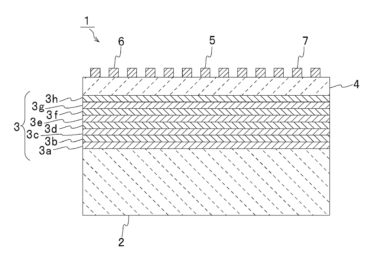
[0035]FIG. 1A is a front cross-sectional view of an elastic wave device according to Preferred Embodiment 1 of the present invention, and FIG. 1B is a schematic plan view illustrating the electrode structure of this device.

[0036]An elastic wave device 1 preferably uses plate waves. The elastic wave device 1 includes a supporting substrate 2. The supporting substrate 2 is preferably made of LiNbO3. The supporting substrate 2 can be made of any material; examples include ceramics, LiTaO3, quartz, Si, glass, and other suitable substances.

[0037]The supporting substrate 2 includes an acoustic reflection layer 3 on top. The acoustic reflection layer 3, in this preferred embodiment, includes high-acoustic-impedance layers 3a, 3c, 3e, and 3g and low-acoustic-impedance layers 3b, 3d, 3f, and 3h. The acoustic impedance of the high-acoustic-impedance layers 3a, 3c, 3e, and 3g is higher than that of the low-acoustic-impedance layers 3b, 3d, 3f, and 3h. In this preferred embodiment, the high-aco...

embodiment 2

[0082]A method for manufacturing an elastic wave device according to Preferred Embodiment 2 starts with preparing the supporting substrate 2. The acoustic reflection layer 3 is then formed on the supporting substrate 2 by a thin-film formation process such as CVD, sputtering, or vapor deposition. The supporting substrate 2 having the acoustic reflection layer 3 on top and a piezoelectric body thicker than the piezoelectric layer 4 are then stuck together by bonding or a similar process. This sticking operation is followed by making the piezoelectric body thinner by polishing, etching, or any other appropriate process to form into the piezoelectric layer 4. After the piezoelectric layer 4 is provided in such a way, the IDT electrode 5 is formed on the piezoelectric layer 4.

[0083]The piezoelectric body can be a single-crystal one so that the piezoelectric layer 4 can have high crystallinity. This improves the resonance characteristics of the elastic wave device 1. It is also possible ...

embodiment 3

[0084]A manufacturing method according to Preferred Embodiment 3 starts with preparing a piezoelectric body thicker than the piezoelectric layer 4. The acoustic reflection layer 3 is then formed on the piezoelectric body by a thin-film formation process such as CVD, sputtering, or vapor deposition. The piezoelectric body having the acoustic reflection layer 3 on either side thereof and the supporting substrate 2 are then bonded together by bonding the substrate to the acoustic reflection layer 3 directly or via a bonding material. The piezoelectric body is then processed and made thinner by polishing, etching, or any other appropriate process to form into the piezoelectric layer 4. Finally, the IDT electrode 5 is formed on the piezoelectric layer 4.

[0085]In this case it is also possible to obtain an elastic wave device 1 with high crystallinity since the piezoelectric body can be a single-crystal one from which a piezoelectric layer having high crystallinity can be formed. Furthermo...


PUM

PropertyMeasurementUnit
acoustic-impedanceaaaaaaaaaa
acoustic impedanceaaaaaaaaaa
piezoelectricaaaaaaaaaa

Abstract

An elastic wave device propagating plate waves includes a stack of an acoustic reflection layer, a piezoelectric layer, and IDT electrode on a supporting substrate. The piezoelectric layer is thinner than a period of fingers of the IDT electrode. The acoustic reflection layer includes low-acoustic-impedance layers and high-acoustic-impedance layers. The low-acoustic-impedance layers are made of SiO2, and the high-acoustic-impedance layers are made of at least one material selected from the group consisting of W, LiTaO3, Al2O3, AlN, LiNbO3, SiN, and ZnO.

Description

BACKGROUND OF THE INVENTION[0001]1. Field of the Invention[0002]The present invention relates to elastic wave devices preferably for use in resonators and band-pass filters and more specifically to an elastic wave device using plate waves and a method for manufacturing the same.[0003]2. Description of the Related Art[0004]Hitherto researchers have proposed elastic wave devices that employ different elastic waves such as Rayleigh waves or SH (shear horizontal) waves. Japanese Unexamined Patent Application Publication No. 2008-530874 discloses an elastic wave device that uses plate waves.[0005]The elastic wave device disclosed in Japanese Unexamined Patent Application Publication No. 2008-530874 has a silicon substrate, an acoustic reflector on the silicon substrate, and a piezoelectric film on the acoustic reflector. IDT (interdigital transducer) electrodes are disposed on the piezoelectric film. The acoustic reflector is a mirror formed of alternately stacked high-elastic-impedance ...

Claims


Application Information

Patent Timeline
Patent Type & Authority Patents(United States)
IPC IPC(8): H03H9/02H01L41/18H03H3/02H01L41/187
CPCH03H9/02535H01L41/18H01L41/1873H03H3/02H03H9/02228H03H9/02574Y10T29/42H10N30/8542H10N30/85
Inventor KIMURA, TETSUYAOGAMI, TAKASHIDAIMON, KATSUYA
Owner MURATA MFG CO LTD
Why Eureka
Try Eureka