

Wafer transport system and method for operating the same
a transport system and a technology for a wafer are applied in the field of a transport system and a method for operating the same, which can solve the problems of easy damage to patterns and active regions, long fabrication time, and many problems, so as to reduce unnecessary movements, prevent the wafer from possible collision, and shorten the fabrication time of the wafer
- Summary
- Abstract
- Description
- Claims
- Application Information
AI Technical Summary
Benefits of technology
Problems solved by technology
Method used
Image

Examples
Embodiment Construction
[0032]In a general aspect, at least one embodiment in accordance with the present invention relates to a wafer transport system and a method for operating the same. More particularly, at least one embodiment relates to a wafer transport system with a low-capacity carrier and a method for operating the same. The embodiments and drawings provided here show different aspects of the present invention. However, the present invention is neither limited to any embodiment nor drawing thereof.
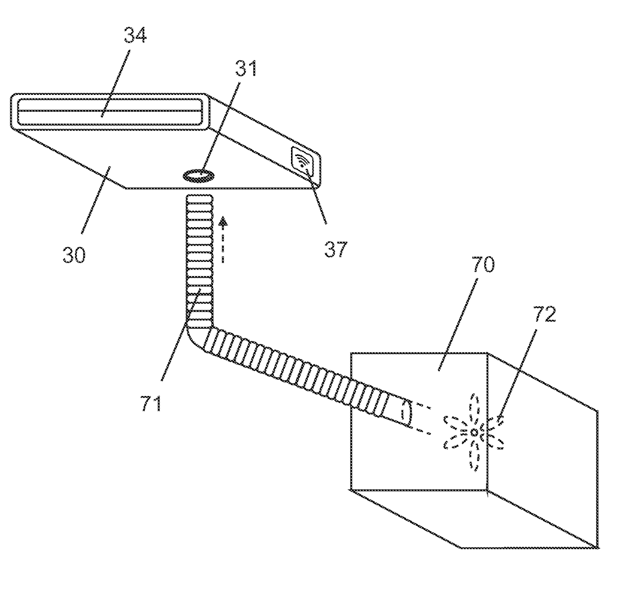
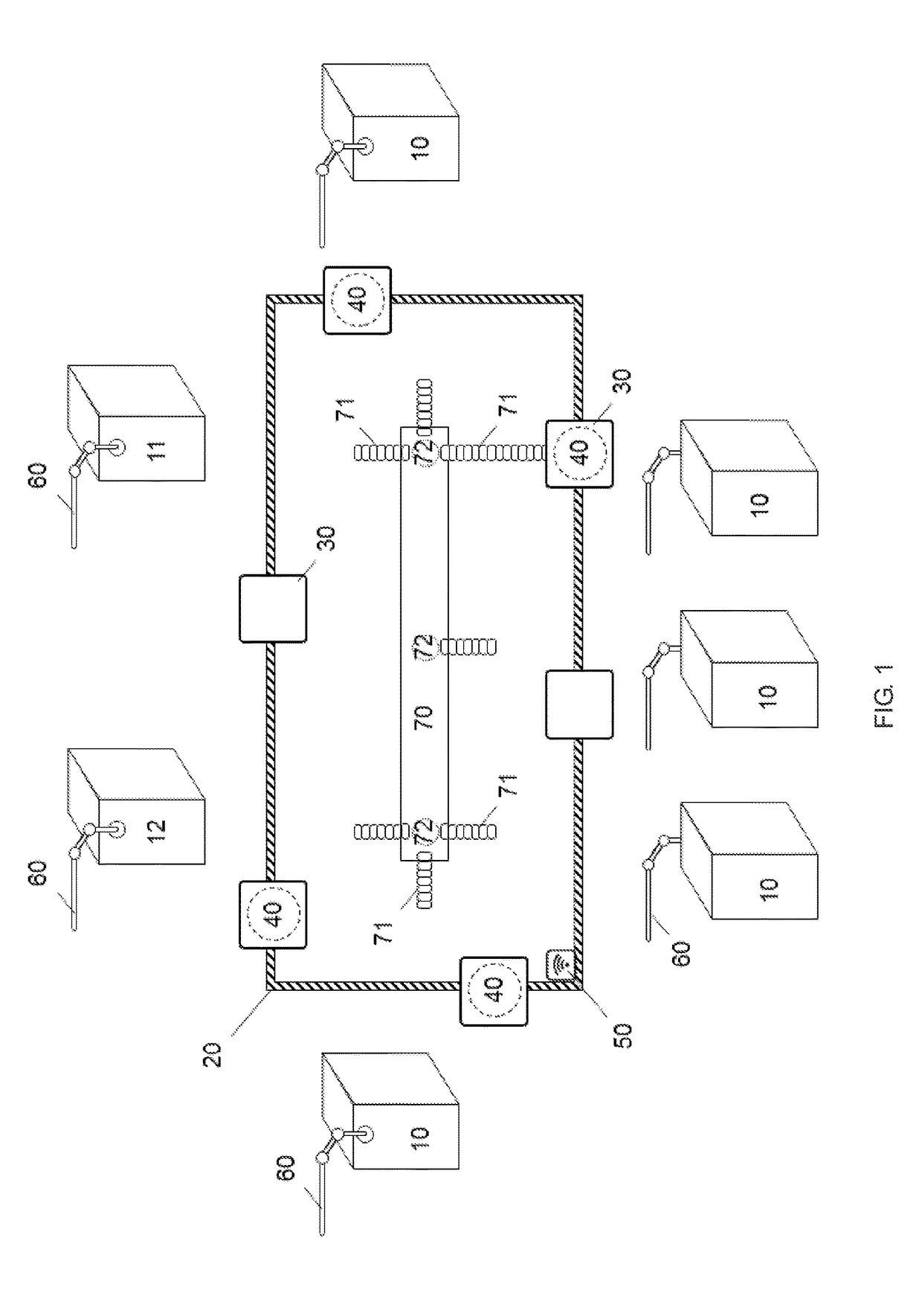
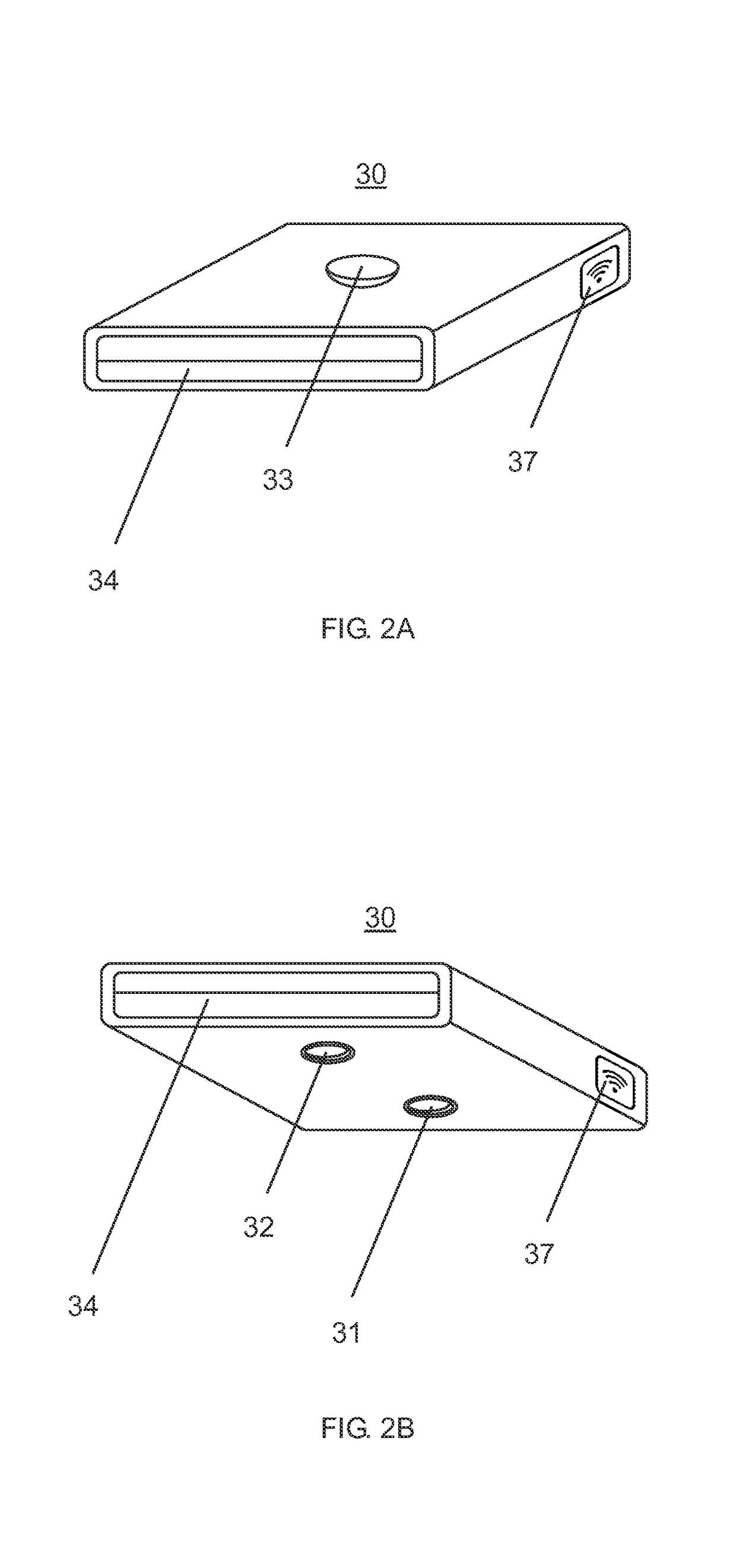
[0033]FIG. 1 is a schematic diagram illustrating an exemplary wafer transport system in accordance with at least one embodiment of the present invention. In FIG. 1, a wafer transport system may comprise at least one semiconductor apparatus 10, an entry port 11, an exit port 12, a track 20, a carrier 30, at least one positioning device 50, at least three transfer devices 60, and a cleaning device 70. The track 20 is located along the at least one semiconductor apparatus 10, the entry port 11, and the exi...
PUM
 Abstract
Description
Claims
Application Information