Titanium silicide realization method in CMOS process by means of titanium deposition at normal temperature

An implementation method and technology of titanium silicide, applied in electrical components, semiconductor/solid-state device manufacturing, circuits, etc., can solve problems such as increasing the leakage current of shallow junctions, and achieve the goal of suppressing narrow channel effects, improving component leakage, and reducing costs. Effect

Active Publication Date: 2007-12-05
SHANGHAI HUAHONG GRACE SEMICON MFG CORP
View PDF3 Cites 0 Cited by
  • Summary
  • Abstract
  • Description
  • Claims
  • Application Information

AI Technical Summary

Problems solved by technology

Amorphization will make the grain size (grain size) of TiSi2 smaller. According to research analysis, reducing the grain size can reduce the temperature or shorten the time required for the process of converting C-49 to C-54, which is equivalent to amplifying The process window is increased (because T1 is reduced), but the amorphization treatment and the increase of the sputtering deposition temperature of Ti are likely to cause junction defects in the CMOS process, which will increase the leakage current of the shallow junction and other adverse effects

Method used


Image

  • Titanium silicide realization method in CMOS process by means of titanium deposition at normal temperature
  • Titanium silicide realization method in CMOS process by means of titanium deposition at normal temperature
  • Titanium silicide realization method in CMOS process by means of titanium deposition at normal temperature

Examples


Embodiment Construction

[0019] The present invention will be further described below with reference to the accompanying drawings and embodiments.

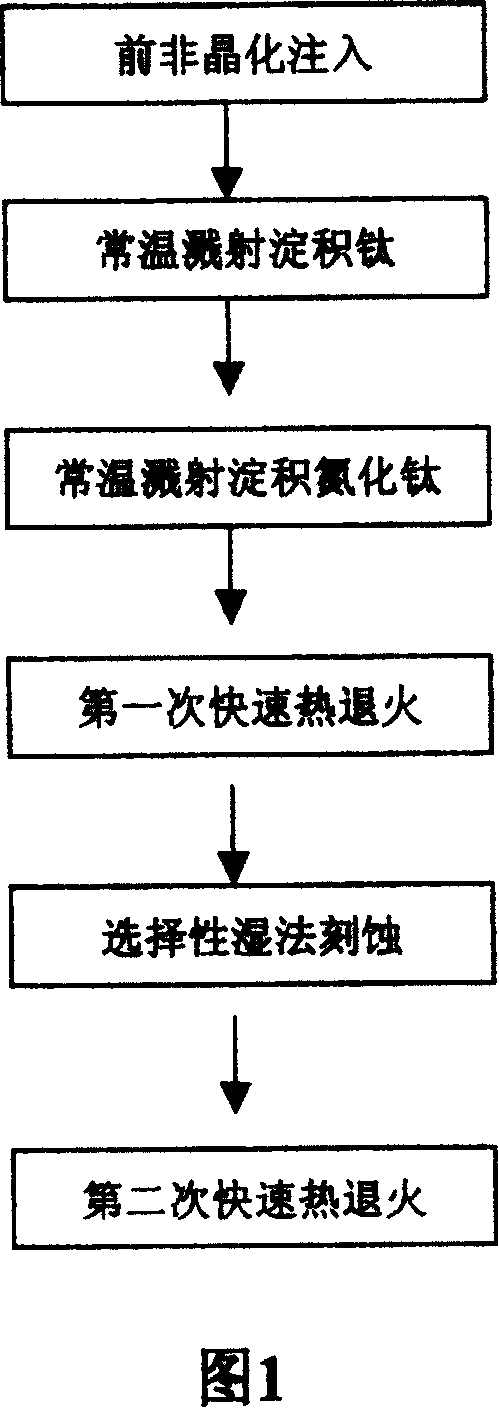
[0020] Referring to FIG. 1 , which is a flow chart of an embodiment of the present invention, a method for realizing titanium silicide by depositing titanium at room temperature in a CMOS process. The following steps:

[0021] Pre-amorphization implantation is performed on the CMOS where the source, drain and gate are formed. As+ implantation is used, and the dose of As+ is 3e14atom / cm3 to amorphize the area where titanium silicide is to be formed, and its energy is equal to The subsequent formation of titanium silicide has a great influence. While not changing the characteristics of the device, optimize its energy to make it the most favorable for the formation of titanium silicide. At the same time, if Ge+ ions are used for implantation, the ideal effect can also be achieved;

[0022] Titanium is deposited by sputtering at room temperature, and titaniu...


PUM


Abstract

The invention relates to realization method for the titanium silicide in CMOS technique, which comprises, first, injecting amorphous compound on CMOS with formed source/drain/grid; then, sputtering to deposit titan at normal temperature for CMOS and adding the sputter and deposit for titanium nitride; annealing quickly for the first time; wet etching by NH4OH/H2O2/H2O; finally, annealing quickly for the second time to form titanium silicide. This method restrains effectively the narrow channel effect, saves time and cost.

Description

technical field [0001] The invention relates to a method for realizing titanium silicide by depositing titanium in a CMOS process, in particular to a method for realizing titanium silicide by depositing titanium at room temperature in a CMOS process. Background technique [0002] In the deep sub-micron semiconductor process, the line width, contact area and junction depth are gradually reduced. In order to effectively improve the working efficiency of the integrated circuit, reduce the resistance and reduce the signal transmission delay caused by the resistance and capacitance (RC), The use of titanium silicides (metal silicides) has become increasingly common. [0003] The Silicide (silicide) process is to deposit a layer of metal (usually Ti, Co or Ni) by sputtering deposition after the gate and source and drain diffusion regions are formed, and after the first rapid annealing ( lst RTA) treatment, the metal and silicon react to form metal silicide, and the metal on the i...

Claims


Application Information

Patent Timeline
Patent Type & Authority Patents(China)
IPC IPC(8): H01L21/8238H01L21/3205H01L21/768
Inventor 马巍金炎陈华伦陈波
Owner SHANGHAI HUAHONG GRACE SEMICON MFG CORP
Why Eureka
Try Eureka