Manufacturing method of polarizing non sensitive semiconductor optical multiplier

A technology of optical amplifier and manufacturing method, applied in instruments, optics, nonlinear optics, etc., can solve the problems of large strain, insensitivity to polarization, etc., and achieve the effect of reducing noise index, easy inversion, and improving performance

Inactive Publication Date: 2007-12-12
INST OF SEMICONDUCTORS - CHINESE ACAD OF SCI
View PDF6 Cites 0 Cited by
  • Summary
  • Abstract
  • Description
  • Claims
  • Application Information

AI Technical Summary

Problems solved by technology

Its disadvantage is that it cannot achieve polarization insensitivity in a large operating current range and wavelength range, and the strain introduced in the tensile strain well is relatively large, and the effect of tensile strain is opposite to the quantum size effect

Method used


Image

  • Manufacturing method of polarizing non sensitive semiconductor optical multiplier
  • Manufacturing method of polarizing non sensitive semiconductor optical multiplier

Examples


Embodiment Construction

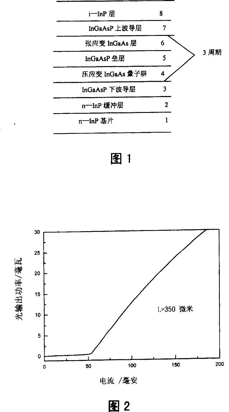
[0032] Please refer to shown in Fig. 1, a kind of preparation method of polarization insensitive semiconductor optical amplifier of the present invention, comprises the steps:

[0033] (1) First grow an epitaxially optimally designed quantum well mixed with quasi-body material on the n-type indium phosphide substrate 1. The active structure specifically includes the buffer layer 2, the lower waveguide layer 3, and the compressive strain quantum well 4. , matched barrier 5, tensile strained quasi-body material 6, in which three identical compressive strain quantum wells and three layers of the same quasi-body material are grown alternately, and the sandwich 5 layers are barriers 5 that are lattice-matched with indium phosphide , and finally the upper waveguide layer 7 and the protective layer 8 are epitaxially grown.

[0034] (2) On the epitaxial sample, grow a layer of silicon dioxide with a thickness of 1500 angstroms as a mask, etch out a strip with a width of 2 μm, and use ...


PUM

PropertyMeasurementUnit
thicknessaaaaaaaaaa
thicknessaaaaaaaaaa

Abstract

The present invention relates to a method for preparing semiconductor optical amplifier with insensitive polarization. Said method is characterized by that on N-type indium phosphide substrate said method adopts three epitaxial process, photoetching process, electrode-making process, cleavage process and anti-reflective film plating process to implement said device preparation.

Description

technical field [0001] The invention is applicable to the technical field of semiconductors, and particularly relates to a method for manufacturing a high-gain broadband polarization-insensitive semiconductor optical amplifier in which compressively strained InGaAs quantum wells and tensile strained InGaAs body materials are alternately grown to form an active structure. Background technique [0002] To make a semiconductor optical amplifier, the device is mainly required to have high signal gain, extremely low polarization sensitivity, large 3dB gain bandwidth, high saturated output power and low noise figure. At present, the 1.55μm semiconductor optical amplifier with good performance mainly adopts the following structures: [0003] 1) Use a nearly square-shaped strain-free body active structure: (see IEEE Photonics Technol. Lett., Vol 6, No. 2; 1994, pp170-172, and pp173-175). The power consumption of the semiconductor optical amplifier with this structure is low, but it...

Claims


Application Information

Patent Timeline
Patent Type & Authority Patents(China)
IPC IPC(8): G02F1/015G02F1/39
Inventor 王书荣王圩刘志宏张瑞英朱洪亮王鲁蜂
Owner INST OF SEMICONDUCTORS - CHINESE ACAD OF SCI
Why Eureka
Try Eureka