Supercharge Your Innovation With Domain-Expert AI Agents!

Method for forming an oxynitride spacer for a metal gate electrode using a PECVD process with a silicon-starving atmosphere

A metal gate and semiconductor technology, applied in semiconductor/solid-state device manufacturing, semiconductor devices, semiconductor/solid-state device components, etc., can solve problems such as low conductivity, poor conductivity, offset, etc.

Inactive Publication Date: 2007-12-12
GLOBALFOUNDRIES INC
View PDF8 Cites 0 Cited by
  • Summary
  • Abstract
  • Description
  • Claims
  • Application Information

AI Technical Summary

Problems solved by technology

[0006] Since many metals are less conductive in the form of their respective metal silicides (formed by the reaction between metal and silicon), if the formation of silicon oxynitride spacers leads to the formation of metal silicides, Advantages of metals as gate materials may disappear or be offset
As the size of the metal gate electrode becomes smaller and smaller, if any part of the metal gate electrode is converted into a less conductive metal silicide, the effectiveness of the metal gate electrode as a conductor becomes less

Method used


Image

  • Method for forming an oxynitride spacer for a metal gate electrode using a PECVD process with a silicon-starving atmosphere
  • Method for forming an oxynitride spacer for a metal gate electrode using a PECVD process with a silicon-starving atmosphere
  • Method for forming an oxynitride spacer for a metal gate electrode using a PECVD process with a silicon-starving atmosphere

Examples


Embodiment Construction

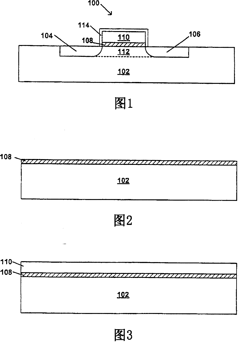
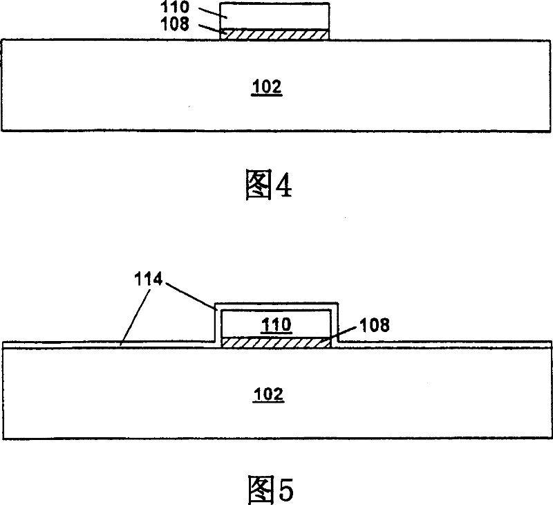
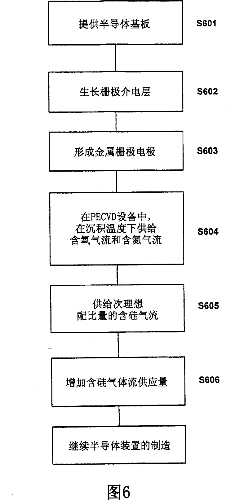
[0017] The term "metal gate" or "metal gate electrode" as used herein refers to the gate or any other Metal structures made of, for example, molybdenum (Mo), nickel (Ni), tantalum (Ta), aluminum (Al), cobalt (Co), copper (Cu), rhenium (Re), titanium (Ti) or tungsten (W) Or a mixture or alloy of two or more metals. The metal may also comprise more than one of tantalum nitride (TaN), tantalum silicon nitride (TaSiN), tungsten nitride (WN), tungsten silicon nitride (WSiN), and similar conductive nitrides of the foregoing metals. As described herein, the metal gate electrode is formed using any method known in the art of fabricating such structures. It should be recognized that although the invention is described herein in terms of a metal gate electrode, the invention is not so limited but extends the scope of the invention to the formation of oxynitrides thereon that reduce or avoid silicide formation. Any metallic structure over a silicon layer.

[0018] The term "silicon ox...


PUM

PropertyMeasurementUnit
refractive indexaaaaaaaaaa

Abstract

A semiconductor device (100) and a method of making the semiconductor device (100) including a metal gate electrode (110), including a semiconductor substrate (102); a metal gate electrode (110); and a silicon oxynitride spacer (114) formed on a surface of the metal gate electrode (110), wherein an interface of the silicon oxynitride spacer (114) and the metal gate electrode (110) is substantially free of metal silicide. The process includes steps of forming a metal gate electrode on a semiconductor substrate; forming by PECVD on a surface of the metal gate electrode a silicon oxynitride spacer, wherein the silicon oxynitride spacer is formed under initially silicon-starved conditions in which a first quantity of at least one silicon-containing material is provided to a PECVD apparatus which is reduced relative to an amount of at least one other reactant, as a result of which substantially no silicide is formed.

Description

technical field [0001] The invention relates to a method of manufacturing a semiconductor device, in particular to a method of manufacturing a dielectric layer on a metal gate of a semiconductor device. Background technique [0002] US-A-4 441 247 discloses a method for fabricating metal oxide semiconductor (MOS) circuits comprising polysilicon components such as metal gates clad with metal. The method comprises the following steps: providing a semiconductor substrate; forming a metal gate on the semiconductor substrate, and forming a silicon oxynitride spacer on the surface of the metal gate by plasma enhanced chemical vapor deposition (PECVD). [0003] As semiconductor devices become more complex, an increasing number of transistors are required on the device. Furthermore, while increasing the speed of devices, their power consumption must be reduced. To solve these problems, the area occupied by each transistor has been greatly reduced. However, it may adversely affect...

Claims


Application Information

Patent Timeline
Patent Type & Authority Patents(China)
IPC IPC(8): H01L21/318H01L21/28H01L29/49C23C16/30H01L21/283H01L21/31H01L21/314H01L21/469H01L21/768H01L23/522H01L29/423H01L29/76H01L29/78H01L29/786
CPCH01L21/28079C23C16/308H01L21/28088H01L21/3145H01L2924/0002H01L21/02274H01L21/0214H01L21/02211H01L2924/00
Inventor M·V·恩戈A·哈里亚
Owner GLOBALFOUNDRIES INC
Features
  • R&D
  • Intellectual Property
  • Life Sciences
  • Materials
  • Tech Scout
  • Unparalleled Data Quality
  • Higher Quality Content
  • 60% Fewer Hallucinations
Learn More