Thin film transistor and its manufacturing method

A technology of a thin film transistor and a manufacturing method, applied in the field of lightly doped drain structures, can solve the problems of low product production rate, LDD structure position shift, complex process and the like

Inactive Publication Date: 2007-12-26
TPO DISPLAY
View PDF5 Cites 0 Cited by
  • Summary
  • Abstract
  • Description
  • Claims
  • Application Information

AI Technical Summary

Problems solved by technology

However, the above method must precisely control the pattern of the gate layer to ensure the location of the LDD structure
Moreover, limited by the photomisalignment of the exposure technology, it is not easy to control the offset of the gate layer, so the problem of the position offset of the LDD structure will be more serious after the two ion implantation processes
Moreover, the process of the above method is complicated, the product production rate is low, and it is not easy to control the lateral length of the LDD structure.
In addition, in terms of circuit design considerations, the conventional technology cannot produce LDD structures of different lengths for different components, so it cannot meet the requirements of reliability and operating speed.

Method used


Image

  • Thin film transistor and its manufacturing method
  • Thin film transistor and its manufacturing method
  • Thin film transistor and its manufacturing method

Examples


no. 1 example

[0047] The first embodiment of the present invention is to manufacture LDD structures of different lengths for TFT components with different operating voltages. By using the lateral length of the gate insulating layer exposed on both sides of the gate layer as a mask and matching an ion implantation process, it can be simultaneously The fabrication of a self-aligned LDD structure and a source / drain region is achieved. The TFT component structure and its manufacturing method of the present invention can be applied to a P-type TFT component or an N-type TFT component, and can be applied to a TFT component in a pixel array area and a peripheral driver circuit area. The following is a detailed description of self-aligned LDD structure and method of manufacture.

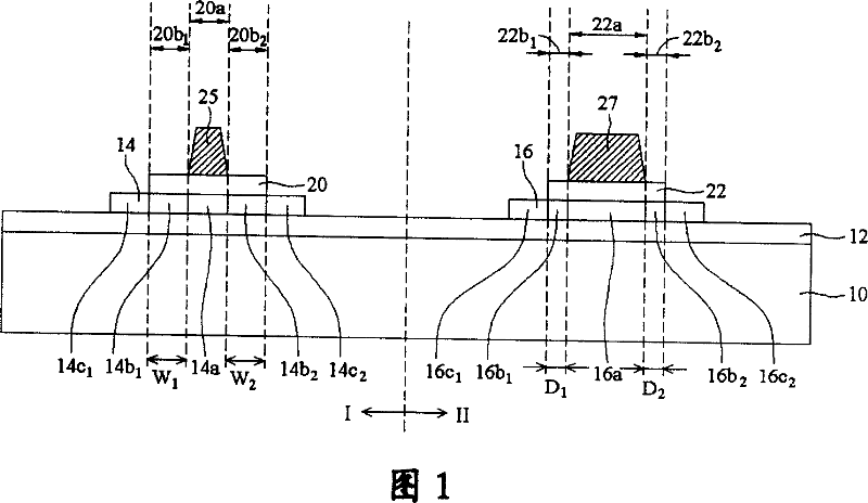
[0048] Please refer to FIG. 1 , which shows a schematic cross-sectional view of a self-aligned LDD structure of a TFT device according to a first embodiment of the present invention.

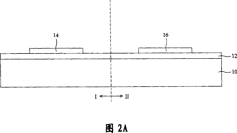
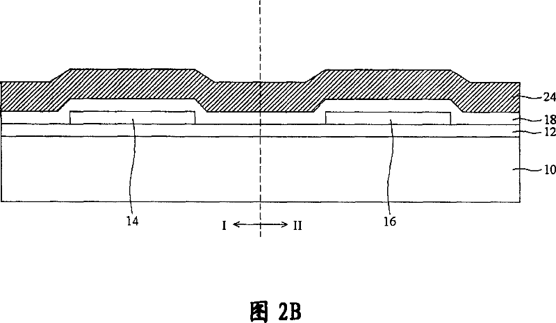
[0049] A substrate 10 includes a fi...

no. 2 example

[0081] Please refer to FIG. 3 , which shows a schematic cross-sectional view of the self-aligned LDD structure of the TFT device according to the second embodiment of the present invention.

[0082] The TFT components and structural features of the second embodiment are substantially the same as those described in the first embodiment, and the similarities will not be described again.

[0083] In the first TFT region I, the first gate insulating layer 20 further includes a first extension region 20c 1 and a second extension region 20c 2 . first extension area 20c 1 is located in the first shielded area 20b 1 left side, and covering the first heavily doped region 14c 1 ; second extension region 20c 2 is located in the second shielded area 20b 2 Right side, and covering the second heavily doped region 14c 2 . In particular, the first extension region 20c 1 Thickness T 1 smaller than the first shielding area 20b 1 Thickness T 2 , it is also possible to make the first ...

no. 3 example

[0087] Please refer to FIG. 4 , which shows a schematic cross-sectional view of a self-aligned LDD structure of a TFT device according to a third embodiment of the present invention.

[0088] The TFT components and structural features of the third embodiment are substantially the same as those described in the second embodiment, and the similarities will not be described again.

[0089] In the first TFT region I, the first gate insulating layer 20 is formed by stacking a first insulating layer 20I and a second insulating layer 20II. The preferred one of the first insulating layer 20I is a silicon oxide layer, a silicon nitride layer, a silicon oxynitride layer or a combination thereof, and the preferred one of the second insulating layer 20II is a silicon oxide layer, a silicon nitride layer , a silicon oxynitride layer or a combination thereof. Located in the central region 20a, the double-layer structure of the first insulating layer 20I and the second insulating layer 20II...


PUM

PropertyMeasurementUnit
Doping concentrationaaaaaaaaaa
Horizontal lengthaaaaaaaaaa

Abstract

The disclosed thin film transistor (TFT) includes following parts and fabricating steps: a first active layer formed on zone of first TFT includes a channel region, a light-doping region and a heavy-doping region; a first grid insulating layer formed on the first active layer includes a central region and a shielding region covering the light-doping region of the first active layer; the second active layer formed zone of second TFT includes a channel region, a light-doping region and a heavy-doping region; a second grid insulating layer formed on second active layer comprises a central region and a shielding region covering the light-doping region of the second active layer; transverse length of shielding region in the first grid insulating layer is not equal to transverse length of shielding region in the second grid insulating layer; transverse length of light-doping region in the first active layer is not equal to transverse length of light-doping region in the second active layer.

Description

technical field [0001] The present invention relates to a thin film transistor (thin film transistor, TFT) technology, in particular to a thin film transistor lightly doped drain (lightly doped drain, LDD) structure technology, which can produce different TFT components for different operating voltages. The LDD structure of asymmetric length can also be fabricated for a TFT device with an asymmetric length. Background technique [0002] The pixel switch component of active matrix liquid crystal display (AMLCD for short) uses a thin film transistor (thin film transistor, TFT), which can generally be divided into two types: amorphous silicon TFT and polysilicon TFT. Due to the higher carrier mobility of polysilicon TFT, better integration of the driving circuit, and smaller leakage current, polysilicon TFT is more often used in circuits with high operating speed, such as: static random access memory (static random access memory) memory, SRAM). However, the polysilicon TFT is...

Claims


Application Information

Patent Timeline
IPC IPC(8): H01L29/786H01L27/11H01L21/336H01L21/8234G02F1/136
Inventor 张世昌方俊雄蔡耀铭
Owner TPO DISPLAY
Why Eureka
Try Eureka