Supercharge Your Innovation With Domain-Expert AI Agents!

3D polysilicon read only memory and preparation method

A technology of read-only memory and manufacturing method, applied in semiconductor/solid-state device manufacturing, electric solid-state devices, semiconductor devices, etc., can solve problems such as the influence of the correct position of the memory cell and the influence of the product qualification rate.

Inactive Publication Date: 2008-01-30
MACRONIX INT CO LTD
View PDF3 Cites 3 Cited by
  • Summary
  • Abstract
  • Description
  • Claims
  • Application Information

AI Technical Summary

Problems solved by technology

In addition, because the region where the electrical breakdown occurs is arbitrary, there is no limited region that can be defined on the interface between the two polysilicon layers, so that the correct position of the memory cell is affected and affects the quality of the product. Pass rate

Method used


Image

  • 3D polysilicon read only memory and preparation method
  • 3D polysilicon read only memory and preparation method
  • 3D polysilicon read only memory and preparation method

Examples


no. 1 example

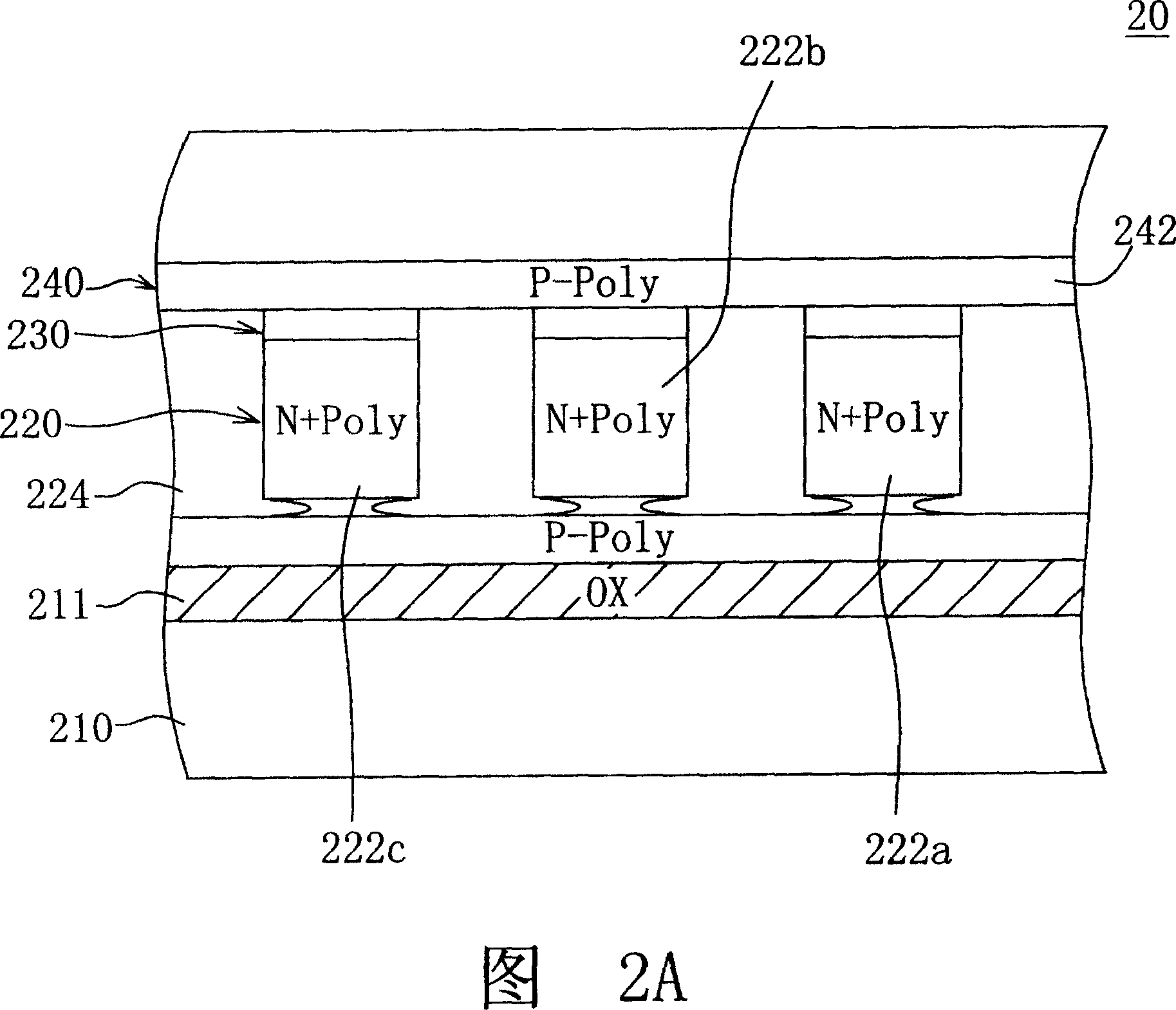
[0018] Please refer to FIG. 2A . FIG. 2A is a cross-sectional view of a three-dimensional polysilicon read-only memory according to a first embodiment of the present invention. The three-dimensional polysilicon ROM 20 includes: a silicon substrate 210 , an insulating oxide layer 211 , an N-type heavily doped polysilicon layer 220 , a P-type lightly doped polysilicon layer 240 , a dielectric layer 230 , and oxide layers 224 and 244 .

[0019] The insulating oxide layer 211 is located on the silicon substrate 210 , and the N-type heavily doped polysilicon layer 220 is located on the insulating oxide layer 211 . The N-type heavily doped polysilicon layer 220 is located on the silicon substrate 210, and the N-type heavily doped polysilicon layer 220 includes several mutually spaced and parallel word lines (Word Line, WL), for the convenience of description, in FIG. 2A , represented by three word lines, which are respectively word lines 222a, 222b, and 222c. The oxide layer 224 is...

no. 2 example

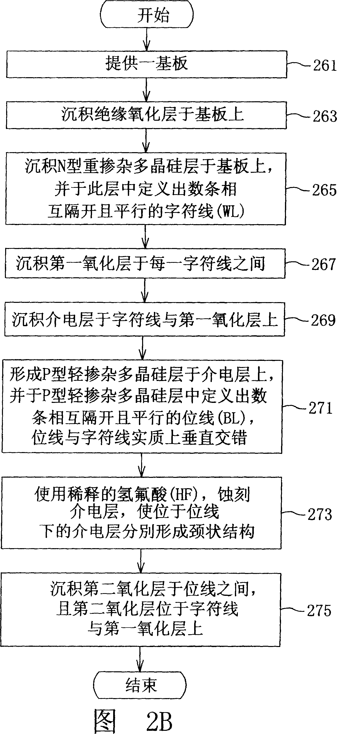
[0027] Please refer to FIG. 3A and FIGS. 3B-3F at the same time. FIG. 3A shows a flow chart of a method for manufacturing a three-dimensional polysilicon read-only memory according to the second embodiment of the present invention, and FIGS. 3B-3F show a flow chart according to the first embodiment of the present invention. A cross-sectional view of the process of the manufacturing method of the three-dimensional polysilicon read-only memory in the second embodiment. As shown in FIG. 3F, the three-dimensional polysilicon read-only memory 30 includes a silicon substrate 310, an insulating oxide layer 311, an N-type heavily doped polysilicon layer 320, a dielectric layer 330, a P-type lightly doped polysilicon layer 340, 350, and an oxide layer 344. , 354.

[0028] The manufacturing method of the 3D polysilicon ROM according to the second embodiment of the present invention is as follows: First, in step 361 , a silicon substrate 310 is provided. Next, in step 363 , an insulatin...


PUM


Abstract

3D polysilicon read only memory includes silicon base plate, insulation oxide layer, N type heavily doped polycrystalline silicon layer, P type light doped polycrystalline silicon layer, dielectric layer and dioxide layer. Insulation oxide layer is on silicon base plate. N type heavily doped polycrystalline silicon layer on insulation oxide layer includes several separated word lines parallel to each other. There is an oxide layer between word lines, and dielectric layer is located on word lines and oxide layer. P type light doped polycrystalline silicon layer on dielectric layer includes several separated bit lines parallel to each other. Bit line is perpendicular to word line, but they are interlaced. A neck structure in dielectric layer is formed under word lines. Another oxide layer positioned between bit lines is located on word lines and first oxide layer.

Description

【Technical field】 [0001] The present invention relates to a read-only memory and its manufacturing method, and in particular to a three-dimensional polysilicon read-only memory and its manufacturing method. 【Background technique】 [0002] Non-volatile memory has the function of "memory". Even after the power is turned off, the data stored in the IC can still be saved. Generally speaking, non-volatile memory can be roughly divided into mask mode read-only memory (MASKROM), one-time programmable read-only memory (OTP ROM), erasable and programmable read-only memory (EPROM), electrically erasable And programmable read-only memory (EEPROM), flash memory (Flash Memory) and multiple times programmable read-only memory (MTP ROM), etc. In the OTP memory array, a fuse is installed on the connecting wire between the transistor and the transistor. When the customer uses the programmer to blow the fuse that is not needed by the OTP to store the program, because the destruction of the ...

Claims


Application Information

Patent Timeline
Patent Type & Authority Patents(China)
IPC IPC(8): H01L27/112H01L21/8246H10B20/00
Inventor 徐子轩李明修龙翔澜吴昭谊
Owner MACRONIX INT CO LTD
Features
  • R&D
  • Intellectual Property
  • Life Sciences
  • Materials
  • Tech Scout
  • Unparalleled Data Quality
  • Higher Quality Content
  • 60% Fewer Hallucinations
Learn More