
LED light source packaging structure for low-temperature coburning ceramic by thermoelectric separating design

A low-temperature co-fired ceramic and LED light source technology, which is applied in the direction of circuits, electrical components, and electrical solid devices, to achieve the effects of simplifying the packaging structure and packaging process, excellent thermal conductivity, and reducing size

Inactive Publication Date: 2008-06-25
长治虹源科技固态显示有限公司
View PDF9 Cites 1 Cited by
  • Summary
  • Abstract
  • Description
  • Claims
  • Application Information

AI Technical Summary

Problems solved by technology

However, none of the above patents discloses the packaging structure of the thermoelectric separation design, nor does it clearly use a dedicated thermal column design in the substrate.

Method used


Image

  • LED light source packaging structure for low-temperature coburning ceramic by thermoelectric separating design
  • LED light source packaging structure for low-temperature coburning ceramic by thermoelectric separating design
  • LED light source packaging structure for low-temperature coburning ceramic by thermoelectric separating design

Examples


Embodiment 1

[0039] Embodiment 1 A packaging structure of a single-chip LED light source using an LTCC substrate

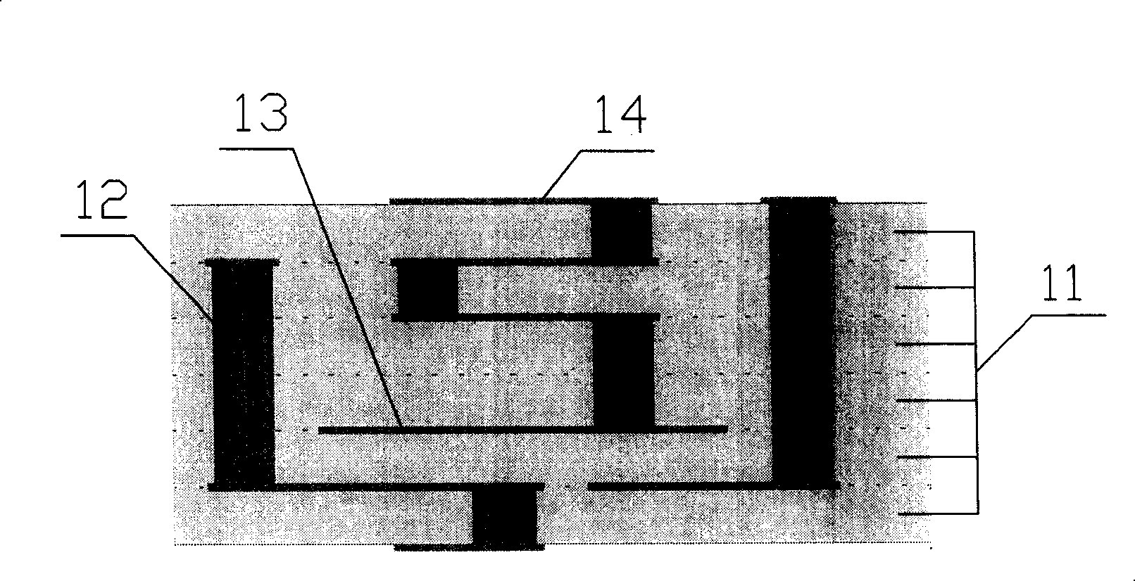
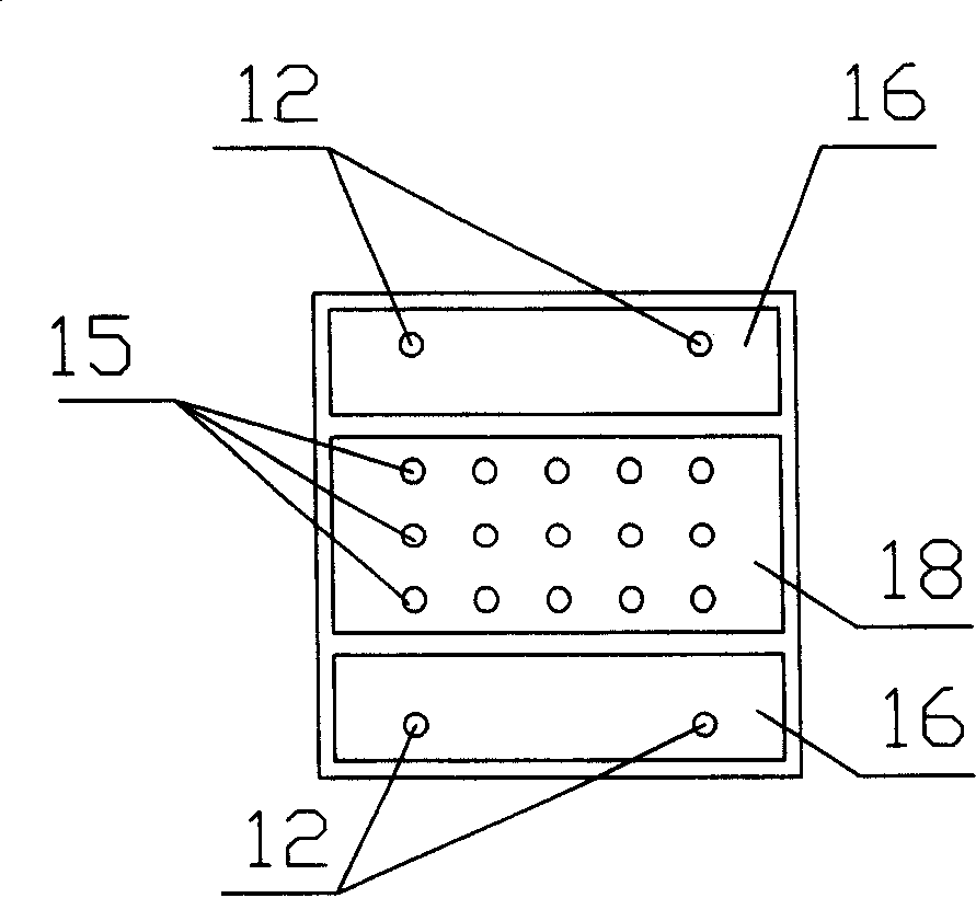
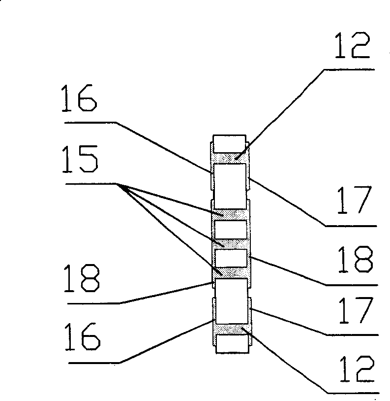
[0040] see Figure 4 , Figure 5 , LTCC substrate 1 is rectangular, and adopts such as figure 2 , 3 The thermoelectric separation structure shown.

[0041] The heat conduction column is filled with silver paste, and the heat generated by the LED chip is transferred to the back of the LED through the silver column.

[0042] Wherein the center of the upper ceramic plate has a cylindrical pit for placing the LED chip 2 .

[0043] The LTCC substrate has produced corresponding circuits and electrodes according to the packaging requirements, and there are 2 electrodes on the back for LED power supply.

[0044] An LED chip 2 is directly fixed on the heat conduction pad in the bottom plane of the substrate pit with high thermal conductivity glue, so that the heat generated by the chip can be quickly transmitted through the LTCC substrate; the power of the LED chip is 1W.

[004...

Embodiment 2

[0047] Embodiment 2 Another packaging structure of a single-chip LED light source using an LTCC substrate

[0048] Basically follow the same steps as in the first embodiment, except that a certain proportion of YAG powder is mixed in the encapsulant 4 , and the YAG powder is excited by a chip that emits light of a specific wavelength to obtain light of a desired color. And glue a lens 5 above the pit of the LTCC substrate, the material of the lens is optical plastic PMMA (acrylic), and it is manufactured by injection molding.

Embodiment 3

[0049] Embodiment 3 A packaging structure of a multi-chip LED light source using an LTCC substrate

[0050] Basically follow the same steps as in Embodiment 1, the difference is that the RGB three-primary color package is used, please refer to Image 6 , that is to use three LED chips, the colors are red, green, and blue, and the working current of the three LED chips is 20mA, and they are fixed together on the plane at the bottom of the same pit on the LTCC substrate; the LTCC substrate has been produced according to the packaging requirements. Corresponding circuits and electrodes enable three LED chips to be independently powered and controlled. There are six electrodes on the back of the LTCC substrate, and each two electrodes independently control a chip.


PUM

PropertyMeasurementUnit
thermal conductivityaaaaaaaaaa

Abstract

The invention provides an LED light source packaging structure of low temperature co-fired ceramic designed by thermoelectric separation, mainly comprising low-temperature co-fired ceramic (LTCC) substrate and LED chip fixed on the substrate, where the top surface of the substrate has pits to hold LED chips; the substrate is a plate in shape, and conducting circuit and heat conducting circuit are mutually independent. And the LTCC substrate uses various ceramic materials as the main, the inner and outer electrodes use Ag, Au, Cu, Ni or other metal, the number of layers and the circuits are determined according to the design requirements. For further improving heat conducting performance, it adopts special heat conducting columns and pads to cool LEDs, thus transferring heat through connected Ag columns to external cooler; and it is applied to multi-chip packaging, able to be used in tricolor or more-color LED packaging. And the invention provides a method for preparing high-brightness LED light source using it.

Description

technical field [0001] The invention relates to semiconductor technology, in particular to the packaging technology of a light emitting diode (Light-Emitting Diode, LED) light source and the low temperature co-fired ceramic (Low Temperature Cofired Ceramic, LTCC) technology; the invention also relates to the packaging preparation method of the light source. technical background [0002] With the advent of ultra-bright LEDs, their efficiency is getting higher and higher, and their prices are gradually falling. At the same time, LED has the characteristics of long life, shock resistance, high luminous efficiency, no interference, no fear of low temperature, no mercury pollution problem and high cost performance. Ultra-high-brightness LEDs have greatly expanded the application of LEDs in various signal display and lighting source fields, mainly including interior and exterior lights of automobiles, various traffic lights, indoor and outdoor information displays and backlights. ...

Claims


Application Information

Patent Timeline
Patent Type & Authority Patents(China)
IPC IPC(8): H01L33/00H01L25/00H01L25/075H01L23/498H01L21/60H01L21/56H01L33/48H01L33/64
CPCH01L2224/45144H01L2224/48091H01L2924/181H01L2924/00014H01L2924/00H01L2924/00012
Inventor 陈盈君
Owner 长治虹源科技固态显示有限公司
Learn More