Flattening active driving TFT matrix structure and method of manufacturing the same

A matrix structure, source-driven technology, applied in semiconductor/solid-state device manufacturing, electrical components, electrical solid-state devices, etc., can solve the problems of easy oxidation or corrosion of the surface, disconnection of metal wires, poor thermal stability, etc. rate, reduce metal wire breakage, and reduce the effect of stress formation

Active Publication Date: 2009-02-18
BEIJING BOE OPTOELECTRONCIS TECH CO LTD +1
View PDF3 Cites 0 Cited by
  • Summary
  • Abstract
  • Description
  • Claims
  • Application Information

AI Technical Summary

Problems solved by technology

However, pure Al and pure Cu still have many disadvantages as electrode materials. One is poor thermal stability, such as the surface of Al film is prone to serious hillock phenomenon after high temperature treatment; the other is poor chemical stability, and the surface is easy to oxidize or corrode.
In order to overcome these shortcomings, the electrode materials used more in large-screen and high-resolution liquid crystal displays are double-layer or multi-layer structures of Al and refractory metals Cr, Mo, etc., but this double-layer or multi-layer structure is greatly improved. The thickness of the gate metal electrode is increased to form obvious steps on the surface of the transparent substrate
This step will bring two problems: one is to bring difficulties to the deposition of the subsequent gate insulating layer, active layer, source-drain metal layer, passivation layer and pixel electrode layer, and make the metal line prone to disconnection, resulting in many bad appearances
Second, this step will inevitably cause a large amount of stress in the subsequent film layers, which is not conducive to the improvement of the yield of the TFT matrix
In order to eliminate the unfavorable factors caused by the steps, various process methods such as two-step wet etching are applied to the preparation of the TFT matrix, but these methods all reduce the slope of the steps and cannot completely eliminate the steps.

Method used


Image

  • Flattening active driving TFT matrix structure and method of manufacturing the same
  • Flattening active driving TFT matrix structure and method of manufacturing the same
  • Flattening active driving TFT matrix structure and method of manufacturing the same

Examples


specific Embodiment 1

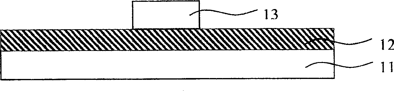
[0033] Figure 1A-Figure 1E The first process method for preparing a planarized TFT matrix structure proposed by the present invention is shown.

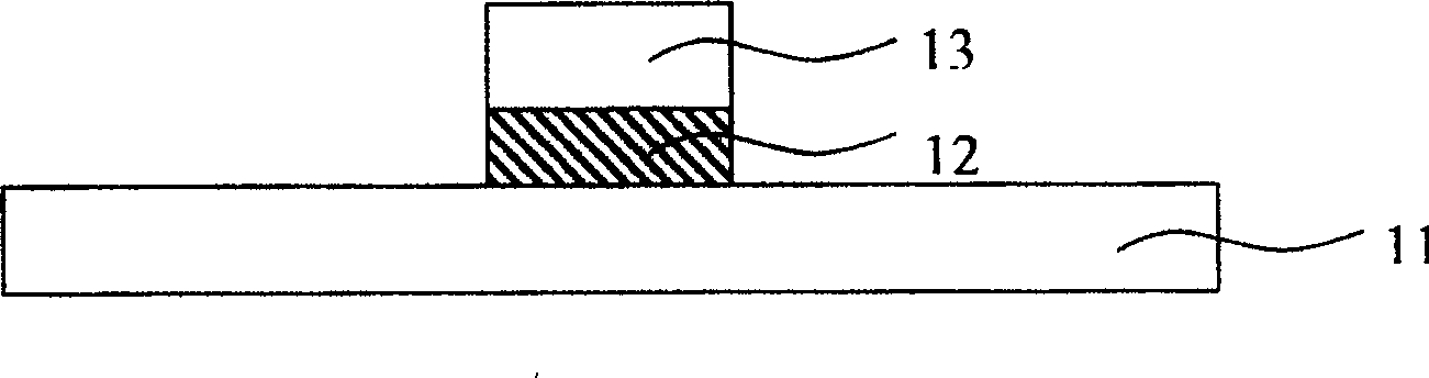
[0034] First, on a transparent glass substrate or quartz 11, use sputtering or thermal evaporation to deposit a thickness of about The gate metal layer 12. The gate metal layer can adopt a single-layer, double-layer or multi-layer structure, and the metal can be selected from Cr, W, Ti, Ta, Mo, Al, Cu and other metals or their alloys. After the gate metal layer is deposited, a photoresist 13 pattern is formed by a traditional photolithography process, wherein the photoresist adopts a positive photoresist, such as Figure 1A . Use wet or dry process to etch away the unnecessary gate metal layer to form gate lines and gate electrodes 16, and at the same time retain the photoresist 13 on the gate lines and gate electrodes 16, such as Figure 1B .

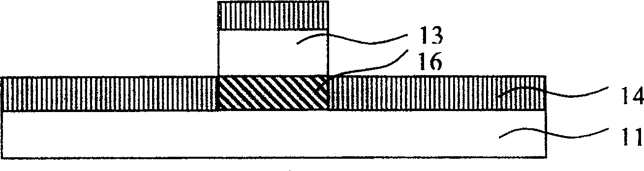
[0035] Secondly, on the transparent glass substrate or quartz 11, photoresist 13, t...


PUM


Abstract

The invention discloses a flat active drive TFT matrix configuration that comprises: base board, grating line, and gate electrode and gate insulation layer, it characterized in that: said grating line and gate electrode are covered onto the base board by the gate insulation layer, the upper surface of the gate insulation layer is flat, semiconductor layer, source electrode and drain electrode and pixel electrode are all formed on the gate insulation layer. The invention also discloses method of producing the flat active drive TFT matrix configuration. The flat insulation surface formed in the invention is propitious to aggradation of later active layer, source and drain metal layer, passivation layer and pixel electrode layer, and reduces the generation of metal fault line. At the same time, flat gate electrode insulation surface can reduce the form of inner stress of the gate insulation layer, and increase the ratio of the finished product.

Description

technical field [0001] The invention relates to an active driving thin film transistor (TFT) matrix structure and a manufacturing method thereof, in particular to a planarized active driving TFT matrix structure and a manufacturing method thereof. Background technique [0002] With the continuous increase of liquid crystal display screens and display pixels, high-resistivity metal materials can no longer meet the requirements of TFT matrix gate signal delay. Therefore, metals with lower resistivity such as Al, Cu, etc. become the first choice for TFT gate metal electrode materials. However, pure Al and pure Cu still have many disadvantages as electrode materials. One is poor thermal stability, such as the surface of Al film is prone to serious hillock phenomenon after high temperature treatment; the other is poor chemical stability, and the surface is easy to oxidize or corrode. In order to overcome these shortcomings, the electrode materials used more in large-screen and h...

Claims


Application Information

Patent Timeline
Patent Type & Authority Patents(China)
IPC IPC(8): H01L27/12H01L21/84
Inventor 王章涛邱海军陈旭闵泰烨林承武
Owner BEIJING BOE OPTOELECTRONCIS TECH CO LTD
Why Eureka
Try Eureka