Split-groove grid flash memory and preparation method thereof

A memory and split slot technology, which is applied in semiconductor/solid-state device manufacturing, semiconductor devices, electric solid-state devices, etc., can solve the problems of NROM flash memory unit area reduction, poor CHEI programming injection efficiency, and limit NROM flash memory, etc., to reduce programming Effects of power consumption, increased scaling capability, and reduced programming power consumption

Inactive Publication Date: 2009-09-02
SEMICONDUCTOR MANUFACTURING INTERNATIONAL (BEIJING) CORP +1
View PDF3 Cites 1 Cited by
  • Summary
  • Abstract
  • Description
  • Claims
  • Application Information

AI Technical Summary

Problems solved by technology

[0005] However, such a conventional planar NROM flash memory of Document 1, such as figure 1 As shown, the proportional reduction of the gate length is still limited by two aspects: (1) In order to suppress the crosstalk between the stored data at both ends of the charge storage layer-silicon nitride and effectively separate two bits of data, the gate length should not be too large. (2) In order to suppress the channel hot electron injection (Channel Hot Electron Injection, CHEI) may cause the source-drain punch-through effect of the unselected cell of the same bit line, it will also limit the reduction of the gate length
These two factors limit the reduction of the unit area of ​​NROM flash memory, which limits the further improvement of storage density; according to the International Semiconductor Technology Development Blueprint (ITRS'2006) in 2006, even at the 35nm technology node, the gate length requirements of NROM flash memory Still greater than 140nm (corresponding to an effective channel length of about 110nm)
At the same time, the CHEI programming of conventional planar NROM flash memory has the disadvantages of poor injection efficiency and high programming power consumption, which also limits the application of NROM flash memory in low power consumption.

Method used


Image

  • Split-groove grid flash memory and preparation method thereof
  • Split-groove grid flash memory and preparation method thereof
  • Split-groove grid flash memory and preparation method thereof

Examples


Embodiment Construction

[0055] The split trench gate flash memory provided by the present invention and its manufacturing method will be described in detail below with reference to the accompanying drawings, but this does not constitute a limitation of the present invention.

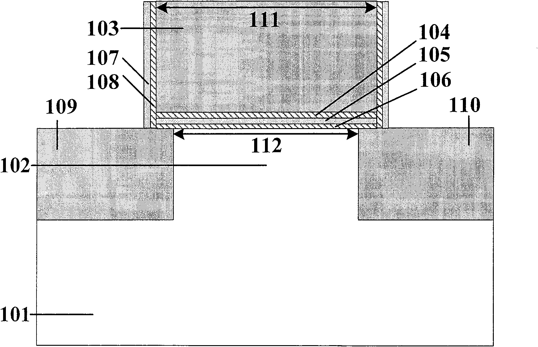
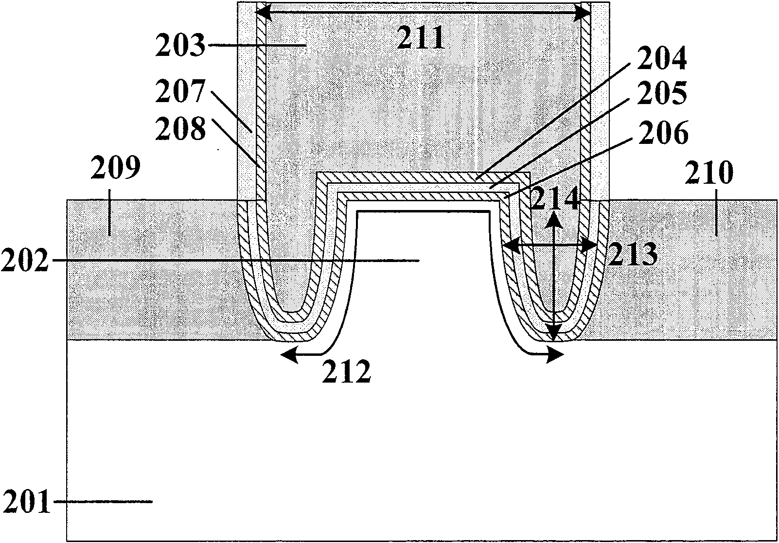
[0056] Such as figure 2 Shown is the split trench gate flash memory of this embodiment. The flash memory is based on a planar structure. In this flash memory, between the two ends of the channel 202 and the n+ source 209 and the n+ drain 210, there is a completely identical trench, the width 213 of the trench is 30nm-40nm, and the depth 214 is 30nm-40nm. 60nm, the trench directly below includes a part of the channel and a part of the n+ source or drain; the channel 202 is divided into three parts, and each of the two ends of the channel has a non-planar channel corresponding to the trench, and the channel In the middle is a planar channel, and a split-recess-channel structure (Split-Recess-Channel) is formed in the channel r...


PUM


Abstract

The invention provides a split trench gate flash memory and a preparation method thereof, which belong to the technical field of non-volatile semiconductor memory in VLSI. The flash memory is based on a planar structure, and there is an identical trench between the two ends of the channel and the n+ source and drain, and the trench directly below includes a part of the channel and a part of the n+ source or drain; The channel is divided into three parts, each of the two ends of the channel has a non-planar channel corresponding to the trench, the middle of the channel is a planar channel, and a split trench gate structure is formed in the channel area; the polysilicon control gate and gate The stack structure completely covers the trench and the channel, and the polysilicon control gate has two protrusions corresponding to the trench; the junction depth of the n+ source and drain is the same as the depth of the trench. The invention can improve the proportional reduction ability of gate length, improve programming injection efficiency and reduce programming power consumption. The preparation method of the present invention is fully compatible with the preparation method of conventional planar NORM flash memory.

Description

technical field [0001] The invention belongs to the technical field of non-volatile semiconductor memory in VLSI, and in particular relates to a split trench gate flash memory and a preparation method thereof. Background technique [0002] Semiconductor memory is an important part of the semiconductor industry. With the increasing demand for data storage in various mobile devices, the demand for non-volatile semiconductor memory that can still store data in the event of power failure is also increasing. A flash memory (Flash Memory, which may be referred to as a flash memory for short) is the fastest-growing non-volatile semiconductor memory. Since the first flash memory product came out in the 1980s, with the development of technology, it has been widely used in mobile communication devices and personal computers such as mobile phones, notebook computers, handheld computers and U disks. Flash memory has captured most of the market share of non-volatile semiconductor memory...

Claims


Application Information

Patent Timeline
Patent Type & Authority Patents(China)
IPC IPC(8): H01L29/792H01L29/423H01L27/115H01L21/336H01L21/28H01L21/8247
Inventor 周发龙吴大可黄如张兴
Owner SEMICONDUCTOR MANUFACTURING INTERNATIONAL (BEIJING) CORP
Why Eureka
Try Eureka