Bare chip building block packaging method

A packaging method and bare chip technology, which is applied in the direction of electrical components, semiconductor/solid-state device manufacturing, circuits, etc., can solve the problems of large volume, complex process, low pass rate and production efficiency, etc., to simplify the process, reduce packaging costs, The effect of reducing the area

Inactive Publication Date: 2007-07-18
徐中祐
View PDF4 Cites 3 Cited by
  • Summary
  • Abstract
  • Description
  • Claims
  • Application Information

AI Technical Summary

Problems solved by technology

[0008] The object of the present invention is to provide a method for packaging multiple integrated circuit bare chips and integrated circuit bare chips for the problems of large volume, complex process, low pass rate and production efficiency in the existing integrated circuit chip packaging technology. A new bare-chip building block packaging method for high-density packaging with other sheet resistors and capacitors and quartz crystal oscillators ( B are-Dies B uilding B lock Technology, BDBB)

Method used


Image

  • Bare chip building block packaging method

Examples


Embodiment 1

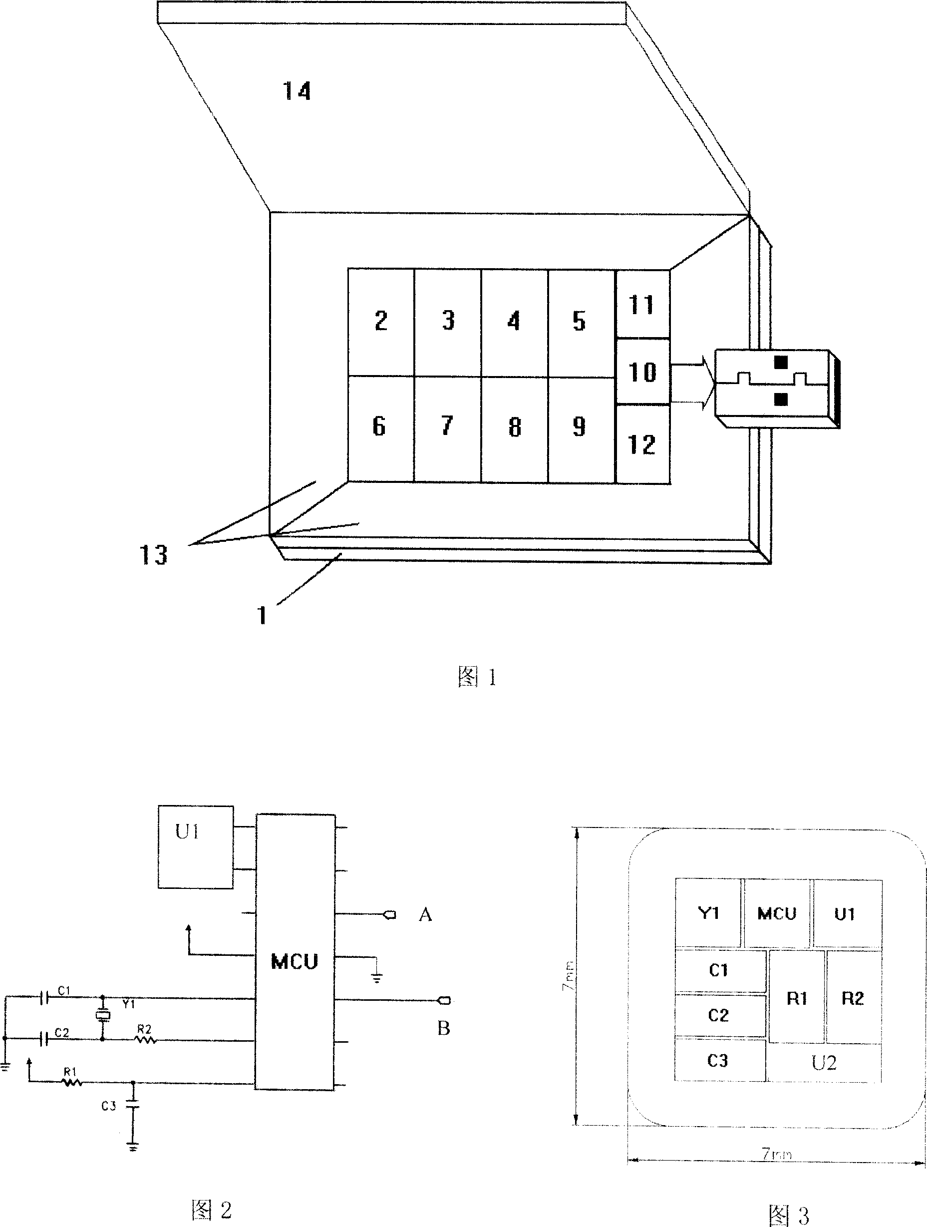
[0039] Embodiment 1: a video storage card with a USB interface.

[0040] The card includes a USB interface chip, a microcontroller chip and eight 512M×8 FLASH memories. Movies can be downloaded from the network through the USB interface and the computer, and stored in the FLASH memory on the card. Then insert the card into a portable MP4 video player and watch it on the go. Adopt the manufacturing process of the present invention as follows (referring to Fig. 1):

[0041] 1) Assemble eight 512M×8 FLASH memory bare chips 2-9, a USB interface control chip 10, and a microcontroller chip 11 into a rectangular matrix as shown in Figure 1, and the blank space without chips is filled with waste Sheet 12, filling waste sheet 12 is filled with waste chips of the same shape, size and thickness as the blank in the blank space without chips to form a square matrix of rectangular silicon chips filled with the same thickness and packed tightly, and placed in a multi-layer printed circuit ...

Embodiment 2

[0048] Embodiment 2: Human heart timing monitor (see Fig. 2 and Fig. 3).

[0049] In order to monitor the heart conditions of patients with coronary heart disease under different activities, patients need to carry complex 24-hour heart monitors, which brings inconvenience to patients when dressing and bathing. The micro-control chip MCU, quartz crystal oscillator Y1, sheet resistors (R1 and R2), sheet capacitors (C1, C2, and C3) and pressure sensor chip U1 required for accurate timing monitoring are made into miniature sheets by adopting the present invention. The 17mm×34mm timing monitoring board produced by the technology is reduced to a micro-sheet with an area of ​​7mm×7mm and a thickness of 1mm, which can be attached to the chest or placed under the skin all year round. Once the patient has symptoms such as myocardial infarction, an alarm signal can be automatically sent. Adopt the manufacture process of the present invention as follows:

[0050] 1) Microcontroller bare...


PUM


Abstract

A modular-packaging method of bare chips includes collecting bare chips to be square array and filling waster chip at blank position, placing said array on base plate of at least 3-layer printed circuit board, cutting out square hole at middle of clamp plate and sheathing said clamp plate at external of square array, covering top plate then setting square array upside down to take off base plate, coating conductive glue at chip back then covering base plate and baking them to form a flat plate, using photo-resist to fill seams, finalizing metal connections and sticking on top plate.

Description

technical field [0001] The invention relates to a new type of integrated circuit packaging module, in particular to a building block packaging method for high-density packaging of multiple integrated circuit bare chips and integrated circuit bare chips with other thin film resistors and capacitors and quartz crystal oscillators. Background technique [0002] The connection between the traditional integrated circuit chip and the chip is realized through the metal wiring of the printed circuit board (PCB). The connection between the semiconductor chip and the printed circuit board usually adopts the following three methods: "bonding" is connected to the metal outer lead frame, packaged with insulating plastic, and then the packaged integrated circuit block is welded to the printed circuit board; 2. The bare chip is directly connected to the printed circuit board through "bonding" 3. Flip-chip welding, that is, the chip is flipped upside down on the printed circuit board, and t...

Claims


Application Information

Patent Timeline
Patent Type & Authority Applications(China)
IPC IPC(8): H01L21/50H01L21/60H01L21/98
Inventor 徐中祐
Owner 徐中祐
Why Eureka
Try Eureka