

High resolution ratio micro optical device parallel direct-writing producing method and producing system
A high-resolution, manufacturing method technology, applied in optical components, semiconductor/solid-state device manufacturing, optics, etc., can solve problems such as slow writing speed, high cost, and low resolution
- Summary
- Abstract
- Description
- Claims
- Application Information
AI Technical Summary
Problems solved by technology
Method used
Image

Examples
Embodiment 1
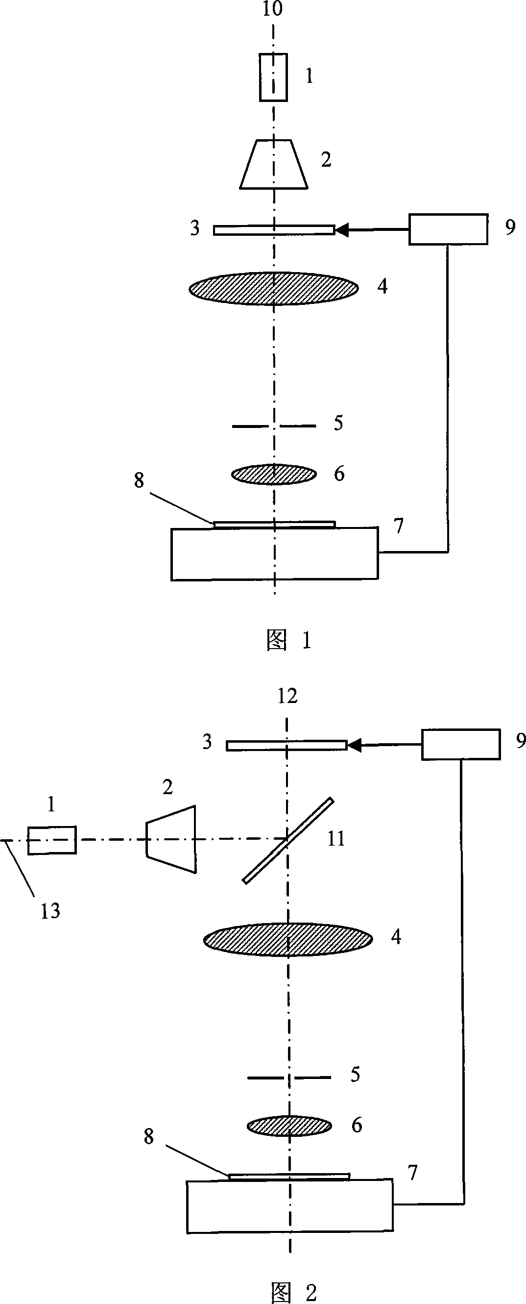
[0051] As shown in Figure 1, the micro-optical device parallel direct writing production system includes a light source 1, a beam expander collimator 2, a transmission-type electrical addressing spatial light modulator 3, a Fourier array on the optical axis 10 in the following order A leaf transformation lens 4, a spatial filter 5, an objective lens 6 and a two-dimensional precision displacement platform 7. Also include the computer 9 that is provided with graphics generation software in the machine, the spatial filter 5 is placed on the rear focal plane of the Fourier transform lens 4, the spatial light modulator 3 is connected with the display video expansion output port of the computer 9 by wires, and Controlled by computer 9 and input graphics signal. The light source 1 is an ultraviolet light source, and may also be a He-Cd laser. The two-dimensional precision displacement platform 7 is connected with the computer 9, and the two-dimensional precision displacement platfor...
Embodiment 2
[0063] As shown in Figure 2, the micro-optical device parallel direct writing production system includes a reflective electrical addressing spatial light modulator 3, a beam splitter 11, a Fourier transform array arranged in sequence on the first optical axis 12 in the following order The lens 4, the spatial filter 5, the objective lens 6 and the two-dimensional precision displacement platform 7 also include the light source 1 and the beam expander collimator 2 on the second optical axis 13, and also include a computer 9 provided with graphics generation software in the machine , the first optical axis 12 and the second optical axis 13 intersect perpendicularly at the beam splitter 11, the angle between the normal of the beam splitter 11 and the two optical axes is 45°, and the spatial filter 5 is placed in the Fourier transform On the rear focal plane of the lens 4, the spatial light modulator 3 is connected with the display video expansion output port of the computer 9 throug...
PUM
 Abstract
Description
Claims
Application Information