Seed and seedholder combinations for high quality growth of large silicon carbide single crystals

A technology of silicon carbide and seed clips, applied in the field of sublimation growth, which can solve the problems of low surface step density per unit area, difficulty, less and more information, etc.

Active Publication Date: 2007-08-29
CREE INC
View PDF2 Cites 27 Cited by
  • Summary
  • Abstract
  • Description
  • Claims
  • Application Information

AI Technical Summary

Problems solved by technology

However, as mentioned above, on-axis growth exhibits less polytype information and a lower density of surface steps per unit area, thus making on-axis growth less effective for replicating multiple polytypes into the growing crystal. relatively difficult technique
[0013] Therefore, for SiC, both on-axis and off-axis seeded sublimation growth techniques exhibit specific disadvantages

Method used


Image

  • Seed and seedholder combinations for high quality growth of large silicon carbide single crystals
  • Seed and seedholder combinations for high quality growth of large silicon carbide single crystals
  • Seed and seedholder combinations for high quality growth of large silicon carbide single crystals

Examples


Embodiment Construction

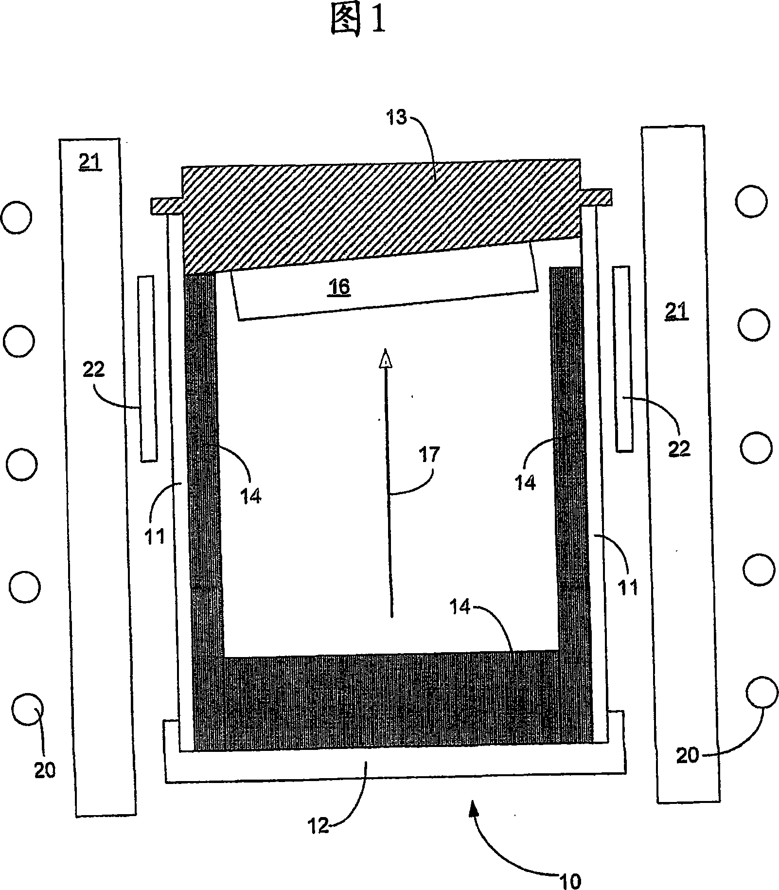
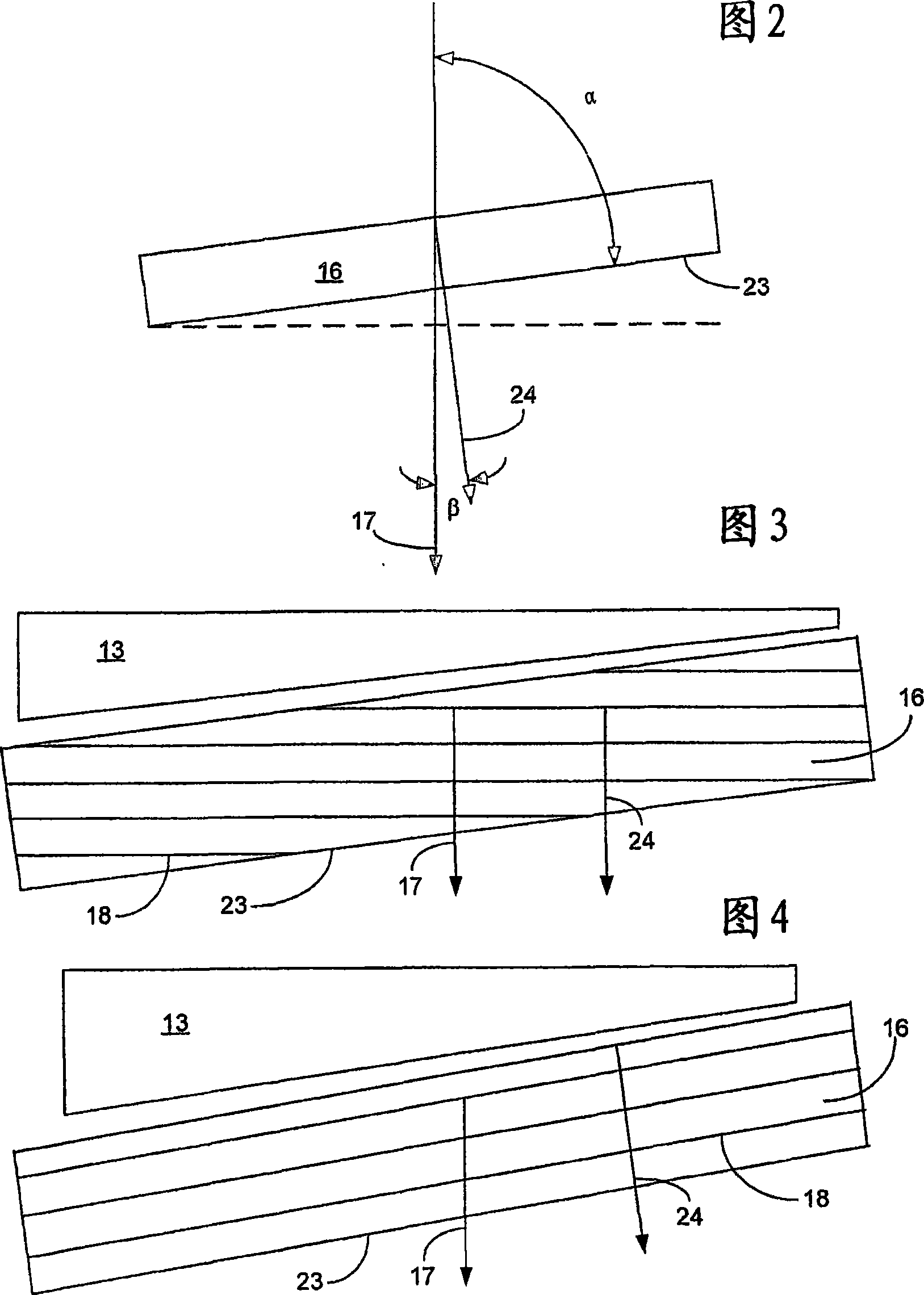
[0027] In a first embodiment, the invention is a seeded sublimation growth system for silicon carbide. In this aspect, the invention includes a crucible, a silicon carbide source composition in the crucible, a seed holder in the crucible, a silicon carbide seed on the seed holder, and means for creating a primary thermal gradient in the crucible , which define the main growth direction between the source composition and the seed to facilitate vapor transport between the source composition and the seed. Place the seed on the seed holder such that the macroscopic growth surface of the seed forms an angle of about 70° to 89.5° with respect to the principal thermal gradient and the principal growth direction, and the crystal orientation of the seed is such that the c-axis of the crystal is aligned with the An angle of about 0° to 2° is formed between the main thermal gradients.

[0028] 1 is a schematic cross-sectional view of a representative seeded silicon carbide sublimation s...


PUM

PropertyMeasurementUnit
melting pointaaaaaaaaaa

Abstract

A silicon carbide seeded sublimation growth system and associated method are disclosed. The system includes a crucible, a silicon carbide source composition in the crucible, a seed holder in the crucible, a silicon carbide seed crystal on the seed holder, means for creating a major thermal gradient in the crucible that defines a major growth direction between the source composition and the seed crystal for encouraging vapor transport between the source composition and the seed crystal, and the seed crystal being positioned on the seed holder with the macroscopic growth surface of the seed crystal forming an angle of between about 70 DEG and 89.5 DEG degrees relative to the major thermal gradient and the major growth direction and with the crystallographic orientation of the seed crystal having the c-axis of the crystal forming an angle with the major thermal gradient of between about 0 DEG and 2 DEG .A silicon carbide seeded sublimation method is disclosed. The method includes the steps of nucleating growth on a seed crystal growth face that is between about 1 DEG and 10 DEG off-axis from the (0001) plane of the seed crystal while establishing a thermal gradient between the seed crystal and a source composition that is substantially perpendicular to the basal plane of the off-axis crystal.

Description

Background of the invention [0001] The present invention relates to the sublimation growth of large single polytype crystals of silicon carbide. [0002] Silicon carbide (SiC) has been known for many years to have excellent physical and electronic properties that theoretically allow fabrication at higher temperatures, higher power and higher frequencies than devices made from silicon or gallium arsenide Electronic devices that work under. About 4×10 6 High breakdown electric field of V / cm, about 2.0×10 7 The high saturation electron drift velocity of cm / s and the high thermal conductivity of about 4.9 W / cm-K make SiC conceptually suitable for high-frequency, high-power applications. [0003] Especially compared with other semiconductor materials, silicon carbide also has a very wide bandgap (for example, the bandgap of α-SiC is 3 electron volts (eV) at 300K, compared with 1.12eV and 1.12eV of Si). GaAs has a band gap of 1.42eV), has high electron mobility, is physically ve...

Claims


Application Information

Patent Timeline
Patent Type & Authority Applications(China)
IPC IPC(8): C30B29/36C30B23/00
CPCC30B23/005Y10S117/911C30B29/36Y10T117/10Y10T117/1032
Inventor S·G·穆勒A·泊韦尔V·F·特斯维特考夫
Owner CREE INC
Why Eureka
Try Eureka