Plasma etching method and computer-readable storage medium

A plasma and etching technology, applied in semiconductor/solid-state device manufacturing, electrical components, circuits, etc., can solve problems such as isotropy, achieve the effect of ensuring etching selectivity and preventing undercutting

Active Publication Date: 2007-09-19
TOKYO ELECTRON LTD
View PDF1 Cites 6 Cited by
  • Summary
  • Abstract
  • Description
  • Claims
  • Application Information

AI Technical Summary

Problems solved by technology

[0006] However, when using NF 3 When the gas etches the etch stop layer made of SiC film, the etching is isotropic, and an undercut (undercut) in which etching proceeds laterally occurs directly under the Low-k film.

Method used


Image

  • Plasma etching method and computer-readable storage medium
  • Plasma etching method and computer-readable storage medium
  • Plasma etching method and computer-readable storage medium

Examples


Embodiment Construction

[0050] Hereinafter, embodiments of the present invention will be described in detail with reference to the drawings.

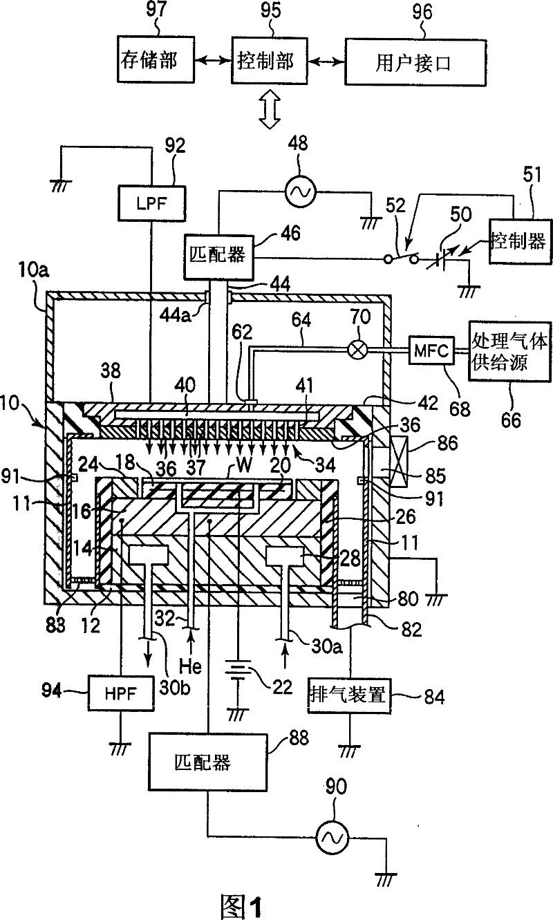
[0051] FIG. 1 is a schematic cross-sectional view showing an example of a plasma etching apparatus used in the practice of the present invention.

[0052] This plasma etching apparatus is configured as a capacitively coupled parallel plate plasma etching apparatus, and has a substantially cylindrical chamber (processing container) 10 made of, for example, aluminum whose surface has been anodized. The chamber (processing vessel) 10 is securely grounded.

[0053] At the bottom of the cavity 10 , a cylindrical base support 14 is disposed via an insulating plate 12 made of ceramics or the like, and a base 16 made of, for example, aluminum is provided on the base support 14 . The susceptor 16 constitutes a lower electrode, and a semiconductor wafer W serving as a substrate to be processed is placed thereon.

[0054]On the upper surface of susceptor 16, electrosta...


PUM


Abstract

In a plasma etching method for plasma-etching an etching stop film after plasma-etching a low-k film in a structure in which a wiring layer, the etching stop film made of an SiC-based material, the low-k film and an etching mask are formed in that order on a substrate, the method includes the step of arranging the structure having the plasma-etched low-k film in a processing chamber in which a first and a second electrode are provided to face each other at vertically separated locations. The plasma etching method further includes the steps of introducing a processing gas containing NF3 into the processing chamber; generating a plasma by applying a high frequency power to one of the first and the second electrode; and applying a DC voltage to said one of the electrodes.

Description

technical field [0001] The present invention relates to a structure after sequentially forming a wiring layer, an etching stopper film made of a SiC material, a low dielectric constant (Low-k) film, and an etching mask on a substrate. A plasma etching method and a computer-readable storage medium for performing plasma etching on an etching barrier film after a low dielectric constant film (Low-k). Background technique [0002] In semiconductor devices, the reduction in wiring intervals due to miniaturization creates large capacitance between wirings, which reduces the signal propagation speed and delays the operating speed. In order to solve this problem, an interlayer insulating film made of an insulating material with a low dielectric constant (Low-k material), that is, a Low-k film, and a multilayer wiring using the film have been developed. On the other hand, copper, which has low electrical resistance and high electromigration resistance, is attracting attention as a w...

Claims


Application Information

Patent Timeline
IPC IPC(8): H01L21/3065
CPCH01L21/31116H01L21/31138H01L21/76804H01L21/7681H01L21/76829
Inventor 吉田亮一
Owner TOKYO ELECTRON LTD
Why Eureka
Try Eureka