Nonvolatile semiconductor memory device
A non-volatile storage and storage device technology, applied in the field of non-volatile semiconductor storage devices, can solve problems such as high write voltage, and achieve the effects of improving water resistance, inhibiting degradation, and improving charge retention characteristics
- Summary
- Abstract
- Description
- Claims
- Application Information
AI Technical Summary
Problems solved by technology
Method used
Image

Examples
Embodiment 1
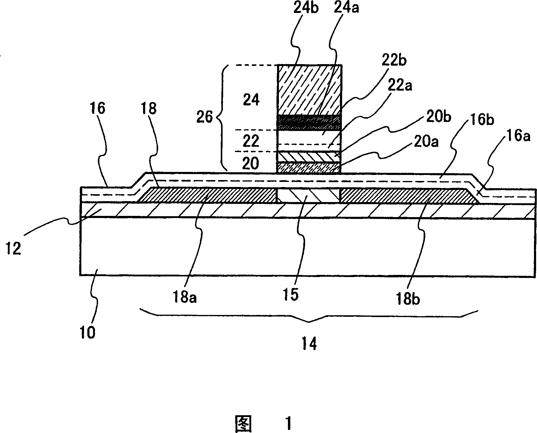
[0134] In this embodiment, an example of a nonvolatile semiconductor memory device will be described with reference to the drawings. Here, a case is shown in which a nonvolatile memory element constituting a memory portion and elements such as transistors constituting a logic portion provided in a nonvolatile semiconductor memory device are formed simultaneously with the memory portion. On the same substrate and perform control of the memory part, etc.
[0135] First, an equivalent circuit of the memory portion of the nonvolatile semiconductor memory device is shown in FIG. 8 .
[0136] In the memory section shown in this embodiment, a plurality of memory cells having selection transistors and nonvolatile memory elements are provided. In FIG. 8, one memory cell is formed by the selection transistor S01 and the nonvolatile memory element M01. Also, like this, the selection transistor S02 and the nonvolatile memory element M02, the selection transistor S03 and the nonvolatile ...
Embodiment 2
[0184] In this embodiment, a case where a plurality of nonvolatile memory elements are provided on one island-shaped semiconductor layer in the structure shown in Embodiment 1 above will be described with reference to the drawings. Note that the same symbols are used for the same parts as those of the above-described embodiment, and descriptions thereof are omitted. FIG. 37 shows a plan view, and FIGS. 38A and 38B show cross-sectional views along lines E-F, G-H in FIG. 37 .
[0185] In the nonvolatile semiconductor memory device shown in this embodiment, there are provided island-shaped semiconductor layers 200a and 200b electrically connected to bit lines BL0 and BL1, respectively, and a plurality of A non-volatile memory element (see FIGS. 37 and 38). Specifically, in the semiconductor layer 200a, a NAND cell 202a including a plurality of nonvolatile memory elements M0 to M31 is provided between the selection transistors S01 and S02. Furthermore, in the semiconductor layer...
Embodiment 3
[0190] In this embodiment, a method of manufacturing a semiconductor device different from that of Embodiment 1 described above will be described with reference to the drawings. Note that the same symbols are used for the same parts as those of the above-described embodiment, and descriptions thereof are omitted. Note that in FIGS. 22A to 24B , A-B and C-D show thin film transistors provided in the logic part, E-F show nonvolatile memory elements provided in the memory part, and G-H show thin film transistors provided in the memory part.
[0191] First, the steps up to FIG. 18C are performed in the same manner as in the above-described embodiment, and then the resist 122 is removed, and the semiconductor layers 104, 106, and 110, the first insulating layer 116 formed on the semiconductor layer 108, and the charge storage layer 121 are covered. The second insulating layer 128 is formed in a stacked structure with the charge storage layer 125 (see FIG. 22A ).
[0192] Next, a r...
PUM
 Abstract
Description
Claims
Application Information
 - R&D Engineer
- R&D Manager
- IP Professional
- Industry Leading Data Capabilities
- Powerful AI technology
- Patent DNA Extraction
Browse by: Latest US Patents, China's latest patents, Technical Efficacy Thesaurus, Application Domain, Technology Topic.
© 2024 PatSnap. All rights reserved.Legal|Privacy policy|Modern Slavery Act Transparency Statement|Sitemap