Self-separation manufacturing method for silicon micro-channel structure

A manufacturing method and technology of silicon microchannels, which are applied in the field of micro-electromechanical systems, can solve problems such as easily damaged back surfaces, and achieve the effects of easy to obtain aspect ratio, high aspect ratio, and easy separation

Inactive Publication Date: 2007-10-17
EAST CHINA NORMAL UNIV
View PDF0 Cites 17 Cited by
  • Summary
  • Abstract
  • Description
  • Claims
  • Application Information

AI Technical Summary

Problems solved by technology

[0006] The invention provides a self-separation manufacturing method of a silicon microchannel plate to solve the problem that the back side is easily damaged in the prior art in the back thinning process

Method used


Image

  • Self-separation manufacturing method for silicon micro-channel structure
  • Self-separation manufacturing method for silicon micro-channel structure

Examples


Embodiment 1

[0031] Embodiment 1, making a silicon microchannel plate for a low-light night vision image intensifier:

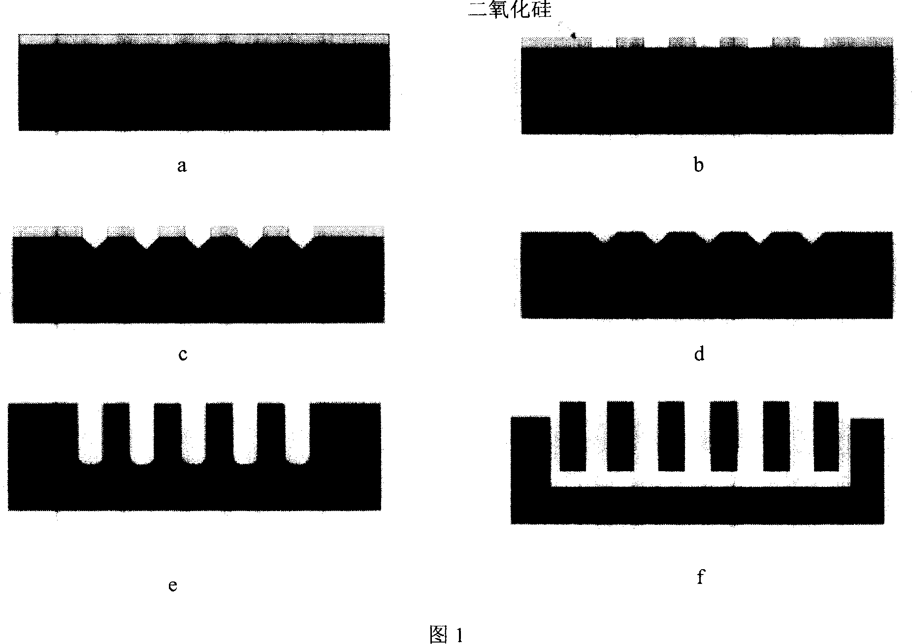
[0032] 1. Select a p-type silicon wafer with a 7-degree inclination in the (100) crystal direction, with a resistivity of 2-5 ohms / cm;

[0033] 2. Using thermal oxidation to form silicon dioxide (sio2) as a mask;

[0034] 3. After defining the window (3μm×3μm) array by photolithography, take it out and clean it; then treat it with tetramethylammonium hydroxide (TMAH 25wt%@80℃) for 1 minute;

[0035] 4. Use buffered hydrofluoric acid (BOE) to corrode for 2 minutes at 37°C;

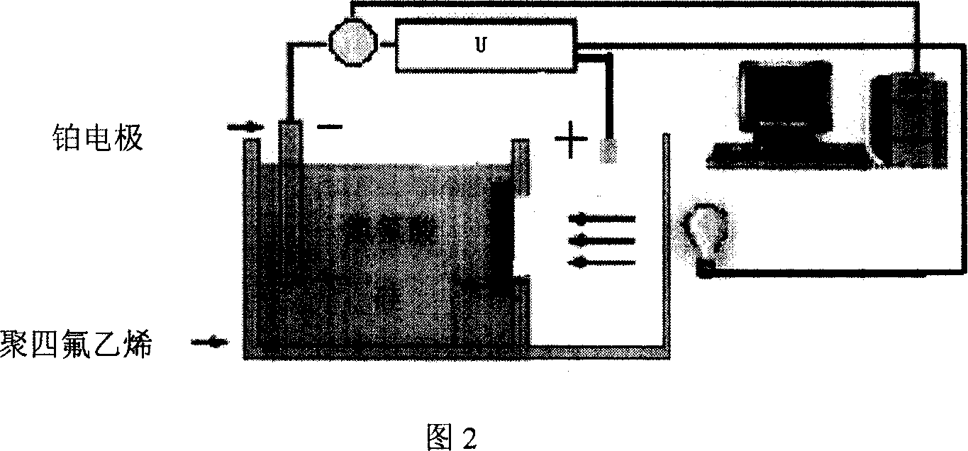
[0036] 5. Rinse and dry with deionized water, then use 40% HF and water to make a 4mol / l solution, and then mix it with tetramethylformamide (DMF) at a ratio of 1:1. After adding the active agent, add Hydrochloric acid (HCl), adjust the pH to 2, the resulting mixed solution is used as an anodic oxidation solution, anodic oxidation is carried out to the treated silicon wafer, anodic oxidation is carri...

Embodiment 2

[0041] Embodiment 2: Microchannel structure for making microbial filter:

[0042] 1. Select p-type silicon wafers in the (100) crystal orientation, with a resistivity of 2-5 ohms / cm;

[0043] 2. Using LPCVD low-stress silicon dioxide (SiO2) as a mask;

[0044] 3. After defining the window (3μm×3μm) array by photolithography, take it out and clean it; then use KOH (40wt%@80℃) for 3 minutes;

[0045] 4. Use buffered hydrofluoric acid (BOE) to corrode for 2 minutes at 37°C

[0046] 5. Rinse and dry with deionized water, then use 40% HF and water to make a 2mol / l solution, and then mix it with tetramethylformamide (DMF) at a ratio of 1:1. After adding the active agent, add Hydrochloric acid (HCl), adjust the pH to 4, and the resulting mixed solution is used as an anodic oxidation solution to anodize the treated silicon wafer. The anodic oxidation is carried out at 20°C, and the average rate of corrosion is 28 μm / h; corrosion 8 Hour;

[0047] 6. Separate the microchannel plate ...


PUM


Abstract

The invention discloses a self-separation preparation method for silicon microchannel structure, which includes steps: 1. pretreatment; 2. electrochemistry process; 3. stripping, concretely containing: a) oxidation / sedimentation for mask; b) photolithography; c) potassium hydroxide corrosion; d) removal of mask; e) deep engraving by electrochemistry; f) microchannel plate peeling. Macropore silicon microchannel prepared by the method possesses high depth-width ratio and is easy to be separated.

Description

technical field [0001] The invention relates to a self-separation manufacturing method of a silicon microchannel structure, in particular to a method for manufacturing a silicon microchannel with a high aspect ratio, and belongs to the field of microelectromechanical system technology (MEMS). Background technique [0002] In the manufacture of devices such as microfluidics, microchannels, and three-dimensional integrated circuits, it is often necessary to make deep hole structures on wafers. Therefore, how to obtain a steep deep hole structure has become one of the focuses in the MEMS process. In order to obtain a relatively steep structure, the existing technologies generally have the following types: [0003] 1. Dry process (deep reactive ion etching, etc.). These methods have achieved success in making sensors of mechanical quantities such as gyroscopes and acceleration sensors. However, there are still many defects, such as: 1. Deep reactive ion etching equipment is v...

Claims


Application Information

Patent Timeline
Patent Type & Authority Applications(China)
IPC IPC(8): B81C1/00B81B1/00
Inventor 王连卫陈晓明林继磊
Owner EAST CHINA NORMAL UNIV
Why Eureka
Try Eureka