Cantilever structure and its making process and application

A manufacturing method and technology of cantilever beams, applied in the direction of microstructure technology, microstructure devices, manufacturing microstructure devices, etc., can solve the problems of increasing device cost, affecting device performance, inconsistent beam thickness, etc., and achieve the improvement of manufacturing yield and processing The process is simple and the effect of improving the control level

Inactive Publication Date: 2007-11-07
SHANGHAI INST OF MICROSYSTEM & INFORMATION TECH CHINESE ACAD OF SCI
View PDF3 Cites 23 Cited by
  • Summary
  • Abstract
  • Description
  • Claims
  • Application Information

AI Technical Summary

Problems solved by technology

[0003] On the making of elastic beam, can adopt the method (L.BruceWilner, Differential capacitive transducer and method of making, US Patent no.4,999,735) of highly doped self-stop corrosion, although described method can control the thickness of beam at In a very small range, but due to the inhomogeneity of doping, the thickness of the beam is inconsistent, and more importantly, doping introduces stress, which will affect the performance of the device
[0004] The combination of dry etching method and wet method is usually carried out in two steps when making elastic beams. First, the pattern of the area where the cantilever beam is located is etched out to obtain a film with the desired thickness of the cantilever beam, and then use Dry etching technology to make elastic beams, such as W.S.Henrion, et.al, Sensors structure with L-shaped spring legs, US Patent No. 5,652,384, this method has difficulties in precisely controlling the thickness of the beams, which increases the complexity of the process, Moreover, expensive equipment is required, which increases the cost of device fabrication
[0005] Using a maskless etching method to form a cantilever beam, such as Jean Hermann et al., micromachinedmeasuring cell with arm supported sensor, US Patent No.555 1294, this method increases the difficulty of controlling the thickness and shape of the cantilever beam

Method used


Image

  • Cantilever structure and its making process and application
  • Cantilever structure and its making process and application
  • Cantilever structure and its making process and application

Examples


Embodiment 1

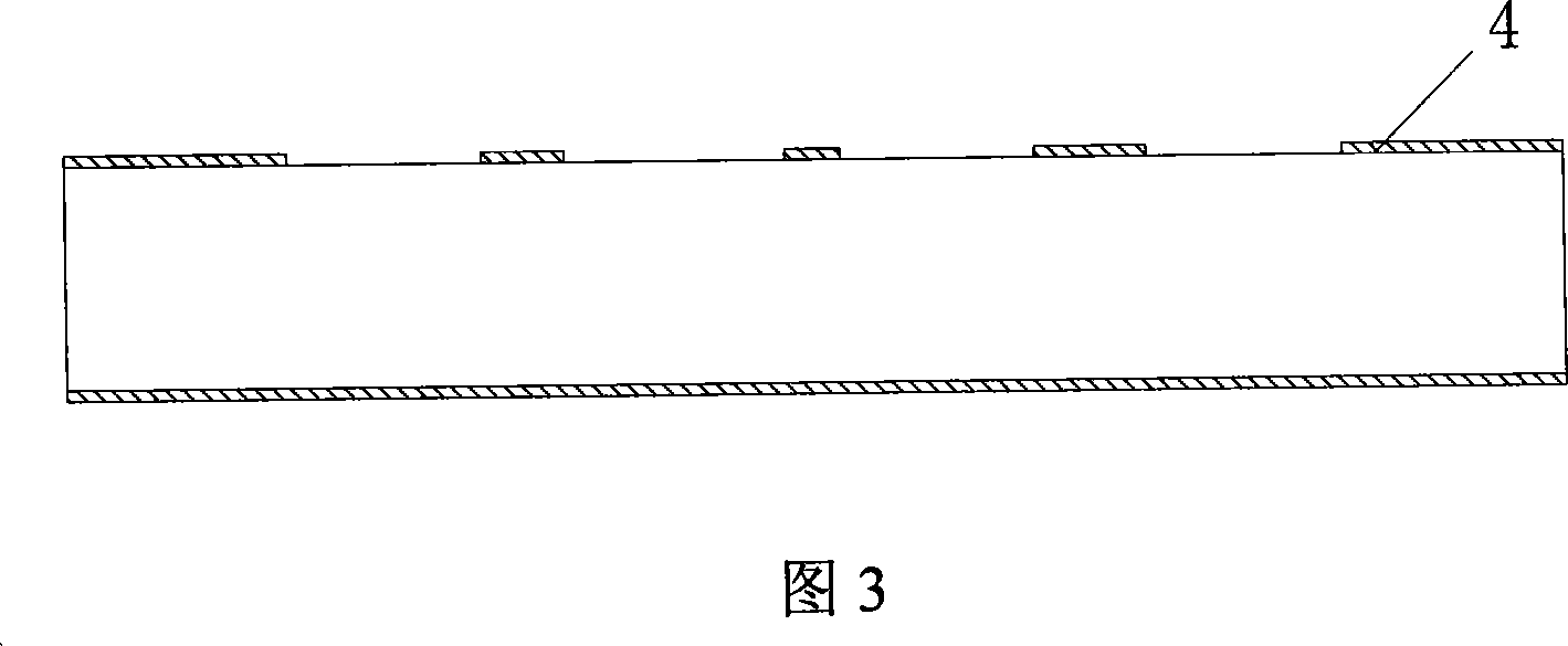
[0046] 1. Use photolithography on the upper surface of the oxidized double-thrown (100) silicon wafer to form a cantilever pattern (Figure 3);

[0047] 2. Etching silicon oxide, performing dry etching of silicon; etching forms the two sides of the cantilever beam (Figure 4);

[0048] 3. On the surface of the silicon wafer after etching, cover a layer of silicon oxide to protect the upper surface and sides of the cantilever beam (Figure 5);

[0049] 4. Perform positive and negative alignment photolithography, and form a silicon etching window on the other side of the silicon wafer, below the cantilever beam (Figure 6);

[0050] 5. Perform anisotropic etching until the two corrosion termination surfaces (111) on the lower surface of the cantilever appear, forming the desired cantilever (FIG. 7).

[0051] The characteristic of this structure is that the lower surface of the cantilever beam will generate two (111) surfaces under the corrosion of the silicon anisotropic etching so...

Embodiment 2

[0052] Embodiment 2 is used to make the elastic beam and mass block of acceleration sensor

[0053] (1) The upper and lower surfaces of the oxidized double-polished (100) silicon wafer are made of damping gap windows by anisotropic etching method, and the etching depth is 4um;

[0054] (2) Secondary oxidation to form silicon oxide, double-sided photolithography, dry etching to obtain 4 straight elastic beams and movable mass at the same time;

[0055] (3) Three times of oxidation, photolithographic pattern on the back, and wet anisotropic etching to obtain straight elastic beams and movable masses at the same time. There are four straight elastic beams on the front side of the silicon wafer, which are distributed on the four corners of the movable mass.

Embodiment 3

[0056] Embodiment 3 is used to make the elastic beam and mass block of acceleration sensor

[0057](1) The upper and lower surfaces of the oxidized double-polished (100) silicon wafer are made of damping gap windows by anisotropic etching method, and the etching depth is 4um;

[0058] (2) Secondary oxidation to form silicon oxide, double-sided photolithography, dry etching on the front and back sides to obtain 8 straight elastic beams and movable mass blocks at the same time;

[0059] (3) Three times of oxidation, photolithographic patterns on the front and back sides, and wet anisotropic etching to obtain straight elastic beams and movable masses at the same time. There are four straight elastic beams on the front and back sides of the silicon wafer respectively, which are distributed on the four corners of the movable mass block.


PUM


Abstract

The present invention relates to cantilever structure manufactured based on the anisotropic silicon etching and its making process, and belongs to the field of microelectronic mechanical system. The present invention features that the cantilever has pentagonal cross section, upper surface of (100) monocrystalline silicon face and lower surface of two (111) monocrystalline silicon faces. The cantilever structure is manufactured through anisotropic etching with the (111) faces as the automatic etching terminating face, and may be controlled precisely to result in high product quality. The present invention may be used in several MEMS devices, such as capacitance type acceleration sensor, resistance type acceleration sensor, micro mechanical gyro, etc for raised device manufacturing control level and device quality.

Description

technical field [0001] The invention relates to a cantilever beam structure and a manufacturing method, more precisely, the invention relates to a cantilever beam structure and a manufacturing method manufactured with silicon anisotropic etching as a key technology. It belongs to the field of microelectromechanical systems. Background technique [0002] Cantilever beams are very important MEMS structural components, and can be applied to the structure of various MEMS devices, such as capacitive acceleration sensors, resistive acceleration sensors, micro-mechanical gyroscopes, resonators, etc. In the past fabrication of cantilever beams, silicon anisotropic wet etching method or dry etching method or a combination of dry etching method and wet method are mostly used. The cantilever beam manufactured by the anisotropic wet etching method of silicon utilizes the characteristics of anisotropic etching of silicon to obtain cantilever beams with various cross-sectional shapes on ...

Claims


Application Information

Patent Timeline
Patent Type & Authority Applications(China)
IPC IPC(8): B81B3/00B81C1/00
Inventor 王跃林车录锋熊斌范克彬
Owner SHANGHAI INST OF MICROSYSTEM & INFORMATION TECH CHINESE ACAD OF SCI
Why Eureka
Try Eureka