Ultrasonic-atomizing heat-decomposing compound semiconductor film preparing system

A technology of thin film preparation and ultrasonic spraying, which is applied in the direction of gaseous chemical plating, metal material coating process, coating, etc., can solve the problems of non-dense film formation, uneven thickness, uneven mixing, etc., and achieve improved stability and improved Purity, the effect of improving film quality

Inactive Publication Date: 2007-11-14
XI AN JIAOTONG UNIV
View PDF1 Cites 19 Cited by
  • Summary
  • Abstract
  • Description
  • Claims
  • Application Information

AI Technical Summary

Problems solved by technology

The common implementation of spray pyrolysis technology is to atomize the solution at the atomization nozzle through high-pressure gas, and spray it directly on the substrate to form a thin film. The disadvantage of this atomization method is that the droplets are large and uneven, and the It is not easy to control, so the surface roughness of the formed film is large, the film is not dense, and generally causes undesirable results such as uneven thickness and thicker center than the surrounding; due to continuous spraying, it is easy to cause insufficient thermal decomposition of the components in the droplet, Influence the quality of film-forming materials (see M.Okuya et al.Solid State Ionics172(2004)527-531)
In some spray coating equipment, the mixing method of carrier gas and mist droplets is too simple and uneven, so it is easy to cause uneven film thickness during the coating process

Method used


Image

  • Ultrasonic-atomizing heat-decomposing compound semiconductor film preparing system
  • Ultrasonic-atomizing heat-decomposing compound semiconductor film preparing system

Examples


example 1

[0030] Example 1, the preparation of ZnO thin film (do not remove air influence)

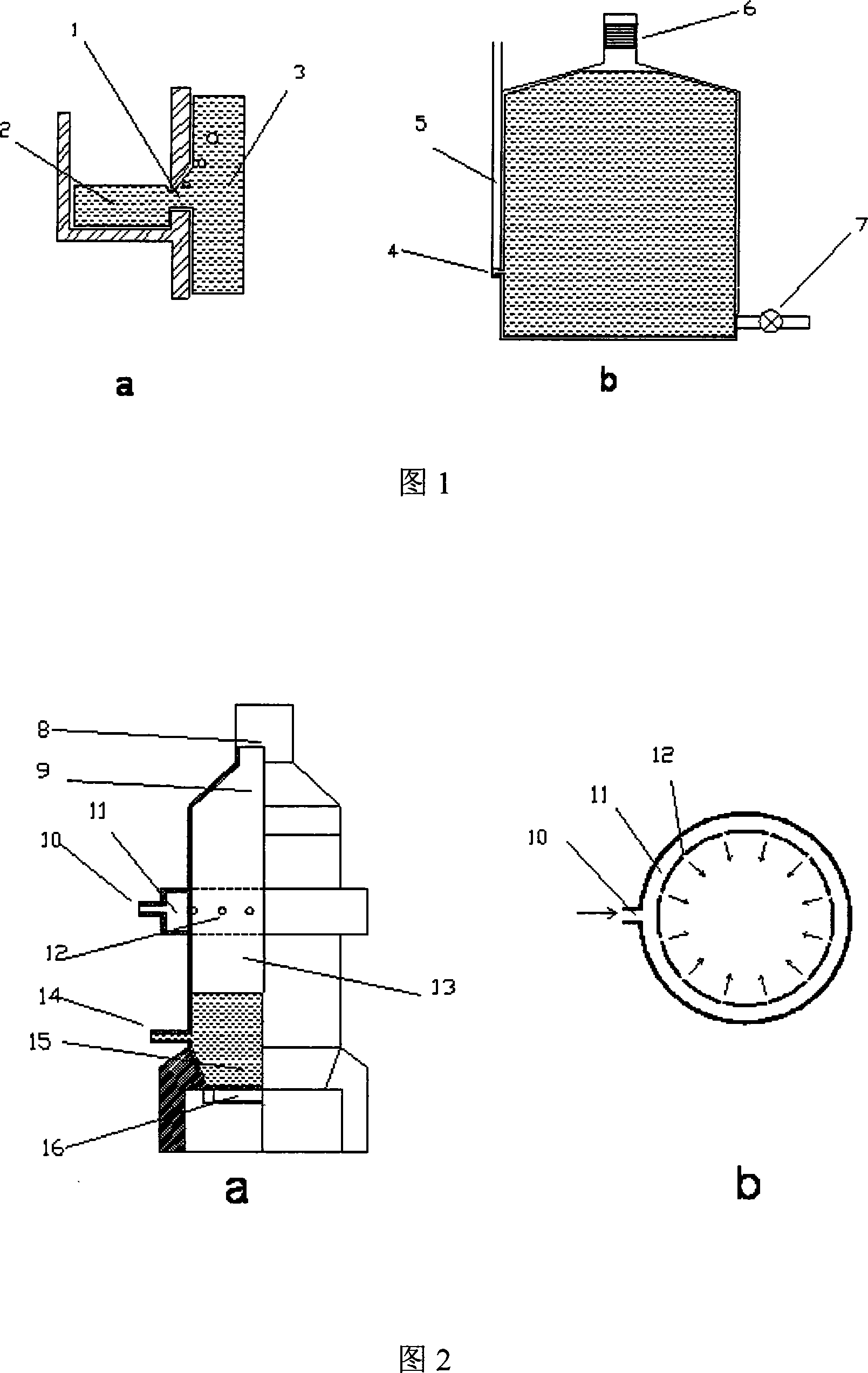
[0031] Preparation of precursor solution: configure 0.05mol L -1 of zinc acetate ((CH3COO) 2 Zn) aqueous solution 200ml. Close the liquid outlet 7 of the liquid storage tank, open the liquid inlet 6, pour in the solution, do not fill it up, and leave a small amount of gas at the top. Seal the liquid inlet 6. After opening the valve 22 of the liquid outlet 7, the solution will flow into the atomization chamber 24, and the liquid level at the upper end of the liquid storage tank 21 will drop to generate a negative pressure. The height of the liquid level (that is, the distance from the atomizing sheet 16 to the liquid level) is 3 cm.

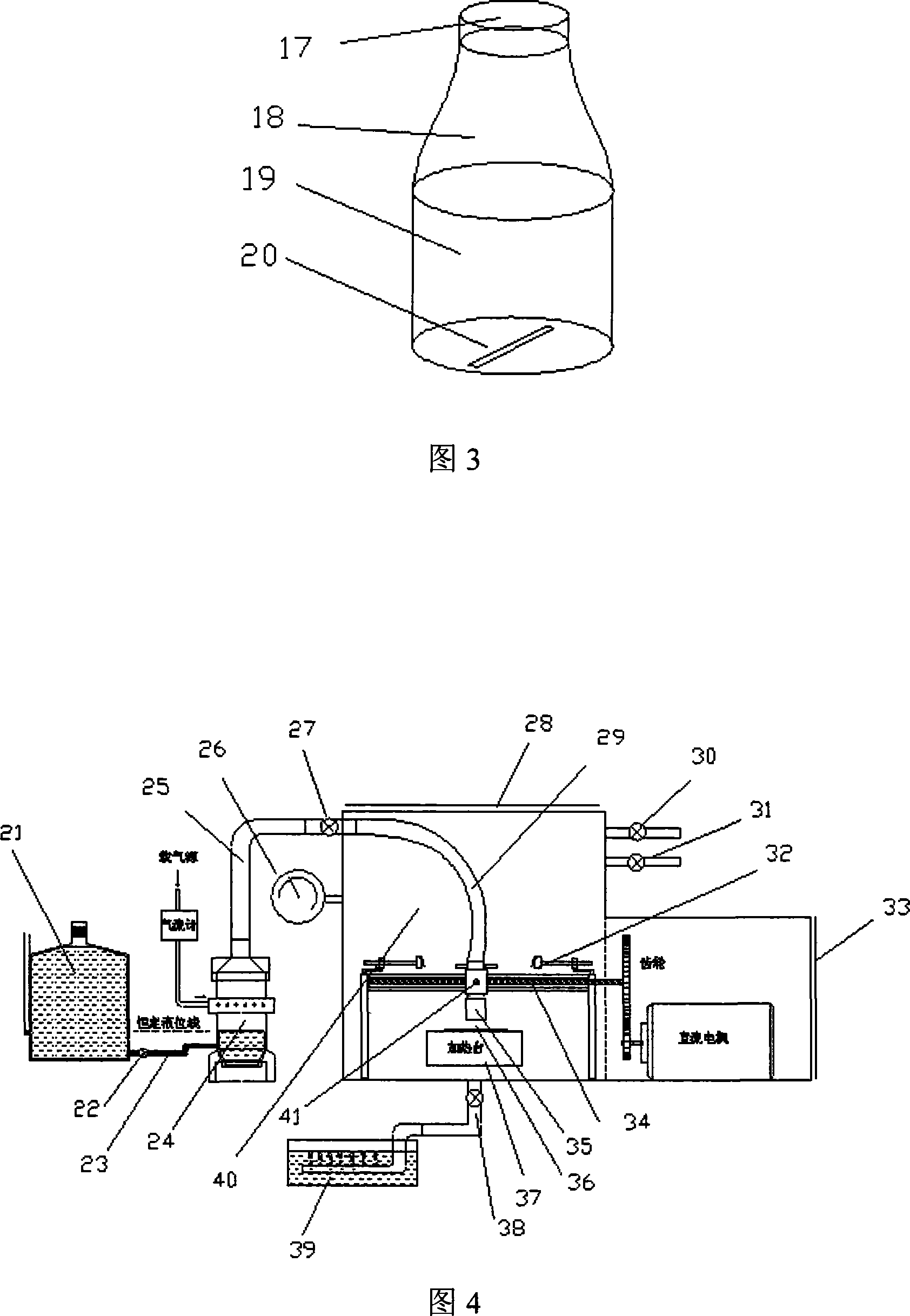
[0032] Thermally decomposed coating: place the substrate 36 (ITO conductive glass, 20 mm×20 mm×1 mm in size) with the conductive side upward on the heating table 37 and fix it. The position of the limit switch 32 is adjusted with reference to the substrate 36 s...

example 2

[0033] Example two, the preparation of CdS thin film (exhausting air to remove the influence of oxygen)

[0034] Preparation of precursor solution: configure cadmium chloride (CdCl 2 ) (concentration is 0.05mol / L) thiourea ((NH 2 ) 2 CS) (concentration of 0.055mol / L (10% excess)) aqueous solution. The process of loading the precursor solution is the same as that of Example 1.

[0035] Air removal: first open the upper operation opening 28 of the deposition chamber 40 to place the substrate 36 and adjust the position of the limit switch 32 in the same manner as Example 1, and then close the upper operation opening 28 of the deposition chamber 40. Close the pumping port 30 and the air inlet 31 valves, open the gas mist inlet 27, the waste gas outlet 38 valves, open the carrier gas, and adjust to a certain flow rate (0.16m 3 / h) Purging the atomization chamber 24 and the aerosol delivery pipe 25 for ten minutes to remove the air in the atomization chamber 24 and the aerosol d...


PUM

PropertyMeasurementUnit
Thicknessaaaaaaaaaa

Abstract

The invention relates to a preparation system of supersonic atomization thermal decomposition compound semiconductor thin film, which is used to prepare the semiconductor thin film of the oxide and the sulfide on the plane matrix. The system consists of atomization and deposit two major parts. Atomization part consists of the carrier gas source, stock solution pot, atomizing chamber and the corresponding electric circuit, while deposit part consists of sealing chamber, spray nozzle, warm table, the electrically operated transmission module, temperature control unit, vacuum manometer, and bubbling pond. Stock solution pot, atomizing chamber, spray nozzle, and sealing chamber are adopted unique design methods. The invention has the merits of cost lowly, operation stable, thin film quality to be good and so on, and the invention can apply to the scientific research and the industrial production of the oxide and the sulfide semiconductor thin film.

Description

technical field [0001] The invention belongs to the field of compound semiconductor thin film preparation and relates to a novel ultrasonic spray thermal decomposition compound thin film preparation system. This system can be applied to the preparation of low-cost and high-quality sulfide and oxide semiconductor thin films. Background technique [0002] Compound semiconductor thin films are widely used in electronic devices, solar cells, functional materials, photoelectrochemical hydrogen production and other fields. However, the preparation of low-cost and high-quality compound semiconductor thin films has always been a difficult problem restricting the development of related scientific research work and industrial technology. At present, the preparation methods of most semiconductor thin film materials are generally methods such as chemical vapor deposition (CVD), magnetron sputtering, vacuum evaporation, etc. These methods are expensive in equipment and make the preparat...

Claims


Application Information

Patent Timeline
IPC IPC(8): C23C16/00C23C16/448
Inventor 郭烈锦苏进展李明涛张西民
Owner XI AN JIAOTONG UNIV
Why Eureka
Try Eureka