

A tunnel probe for scanning the tunnel microscope and its making method
A technology of scanning tunneling and microscopy, applied in the field of tunneling probes, can solve the problems of difficult manufacturing process and difficult to obtain high-resolution tunneling probes, and achieve the effect of improving resolution
- Summary
- Abstract
- Description
- Claims
- Application Information
AI Technical Summary
Problems solved by technology
Method used
Image

Examples
Embodiment 1
[0046] Embodiment 1, preparation of high-resolution metal W tunnel probe
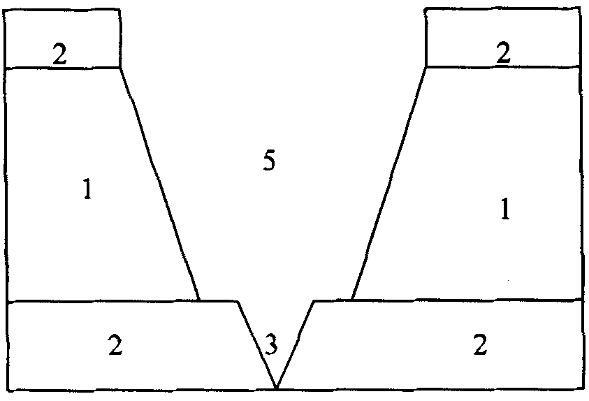
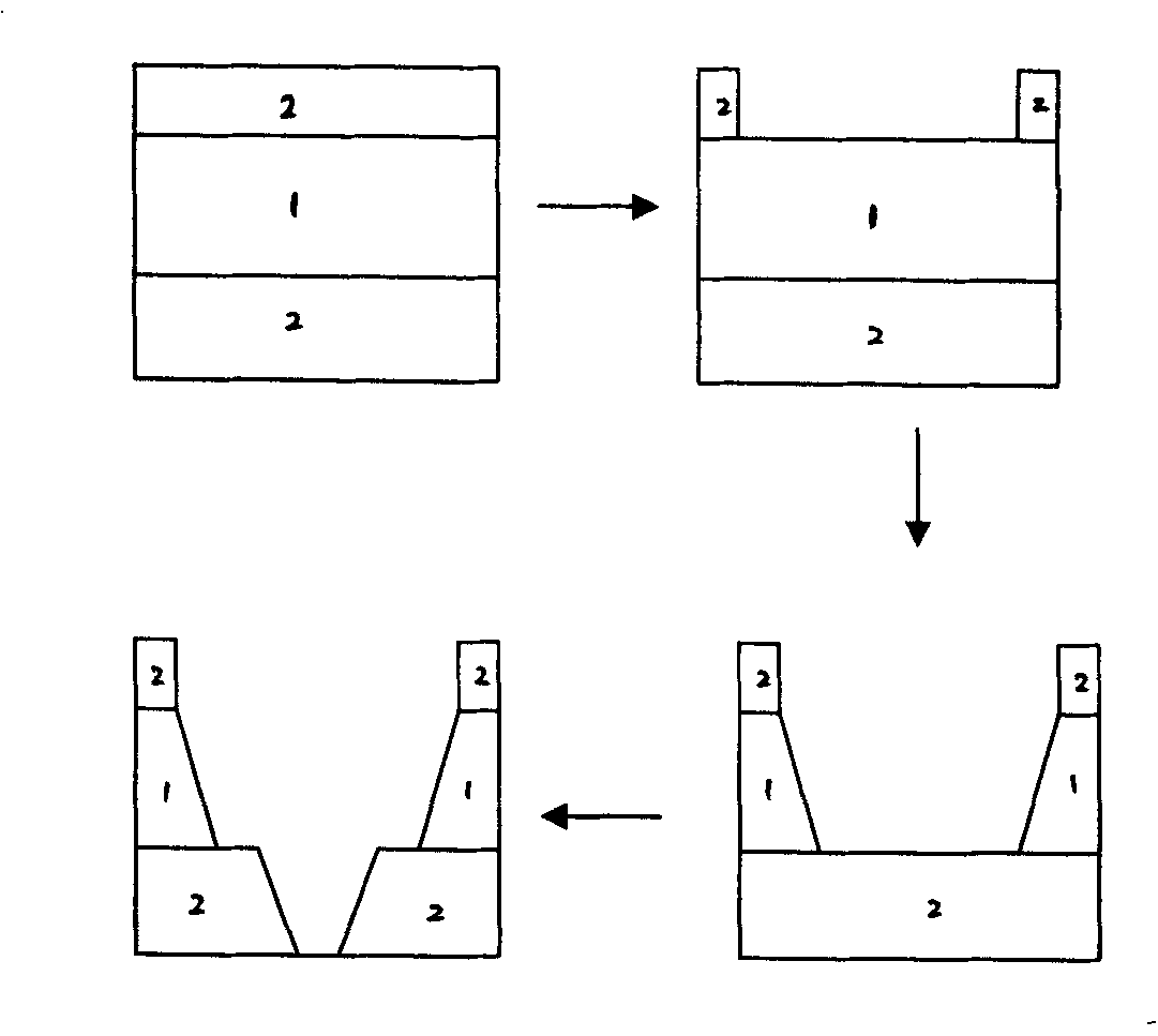
[0047] On both sides of the Si(100) substrate 1, a 100-nm-thick SiN film 2 was prepared by chemical vapor deposition (CVD), and then a window of 0.2×0.2 square millimeters was opened on one side by ultraviolet lithography. , using chemical reaction etching to remove the SiN film in the window. Put the sample into 65°C, 4M KOH solution for etching. Since the rate of etching Si by KOH solution is much higher than that of etching SiN, it is obtained as follows figure 2 As shown in , there is a SiN film with a window etched on one side of the Si substrate, and there is also a 0.2×0.2 square millimeter window in the center of the Si substrate. The Si substrates on both sides serve as supports for the SiN film on the other side. To ensure that the SiN film at the window is not broken, and at the same time facilitate the processing of the sample.
[0048] Using the focused ion beam (FIB) etching method, on ...
Embodiment 2
[0050] Example 2. Preparation of high-resolution ferromagnetic metallic Co spin-polarized tunneling probes
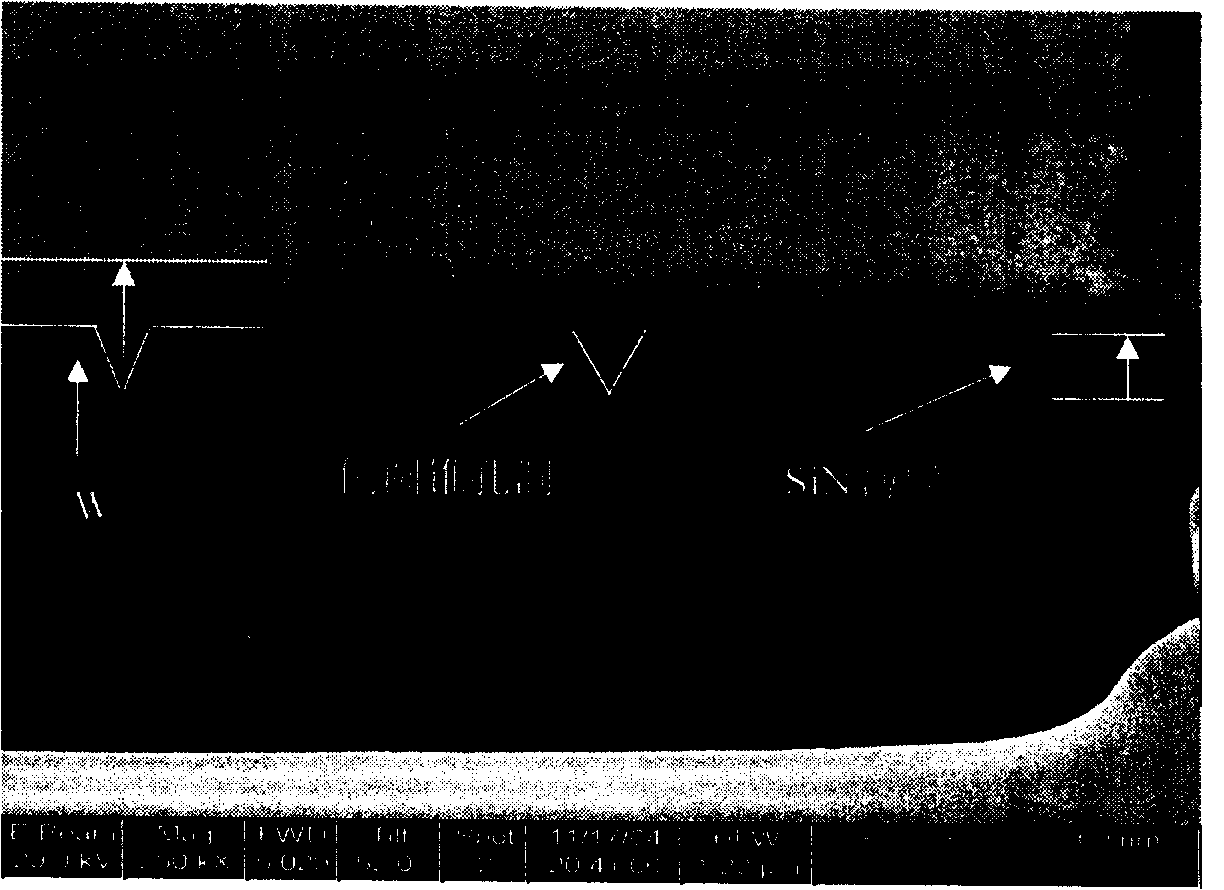
[0051] Using the focused ion beam (FIB) etching method, on the 100nm thick SiN insulating layer described in Example 1, prepare a rounded frustum-shaped hole with a diameter of 40 nanometers on the upper surface and a diameter of 3 nanometers on the lower surface. The conditions are as follows: ion acceleration voltage 30KV, ion beam current 10PA, ion point residence time 30μs, ion beam minimum step size 5nm, ion beam emission current 22μA, sample chamber vacuum 3×10 -5 Pa, the etching time is 0.3 seconds, and a rounded truncated hole with a diameter of 40 nanometers on the upper surface and a diameter of 3 nanometers on the lower surface can be obtained on the SiN insulating layer.
[0052] Then use molecular beam epitaxy to deposit ferromagnetic metal Co on the SiN substrate with rounded frustum-shaped holes, the deposition conditions are: system vacuum 3 × 10 -10 Pa...
Embodiment 3
[0053] Embodiment 3, prepare high-resolution semimetallic CrO 2 High Spin Polarization Tunneling Probe
[0054] Using the focused ion beam (FIB) etching method, on the 100nm thick SiN insulating layer described in embodiment 1, prepare the hole that the upper surface diameter is 20 nanometers, the lower surface diameter is 1 nanometer round frustum shape, etch The conditions are as follows: the ion acceleration voltage is 30KV, the ion beam current is 10PA, the ion point residence time is 30μs, the minimum ion beam step size is 5nm, the ion beam emission current is 22μA, and the vacuum degree of the sample chamber is 3×10 -5 Pa, the etching time is 0.2 seconds, and a rounded frustum-shaped hole with a diameter of 20 nanometers on the upper surface and a diameter of 1 nanometer on the lower surface can be obtained on the SiN insulating layer.
[0055] The semimetallic CrO was then deposited on the SiN substrate with rounded frustum-shaped holes using a laser pulse deposition m...
PUM
| Property | Measurement | Unit |
|---|---|---|
| diameter | aaaaa | aaaaa |
| diameter | aaaaa | aaaaa |
| thickness | aaaaa | aaaaa |
Abstract
Description
Claims
Application Information