Silicon of insulator and its making technology

A silicon-on-insulator and preparation technology, which is applied in semiconductor/solid-state device manufacturing, electrical solid-state devices, semiconductor devices, etc., can solve the problems of small thickness of top silicon, small thickness of buried insulating layer, poor adjustability, etc., and achieve improvement Performance, reduction of direct impact, and effect of improving performance

Inactive Publication Date: 2008-01-09
SHANGHAI SIMGUI TECH +1
View PDF1 Cites 14 Cited by
  • Summary
  • Abstract
  • Description
  • Claims
  • Application Information

AI Technical Summary

Problems solved by technology

Although the silicon-on-insulator prepared by the above-mentioned process has better insulation performance of the buried insulating layer, since the buried insulating layer is formed by ion implantation, the thickness of the buried insulating layer is small due to the limited energy of ion implantation. , the adjustable range is also small; and the thickness of the top silicon is also small, and the adjustability is poor

Method used


Image

  • Silicon of insulator and its making technology
  • Silicon of insulator and its making technology
  • Silicon of insulator and its making technology

Examples


Embodiment 1

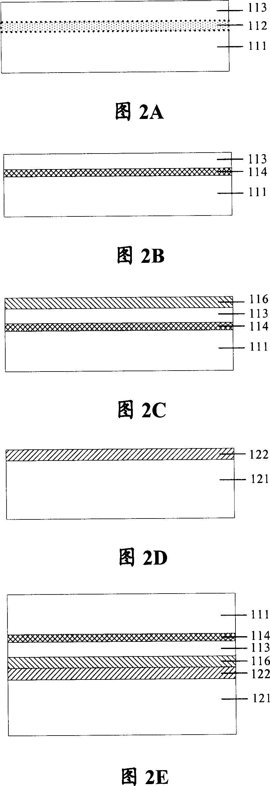
[0079] In this embodiment, the surface silicon layer is the first surface silicon layer 113 shown in FIGS. 2A to 2I , and the insulating layer is the first insulating layer 116 .

[0080] Referring to FIG. 2A, it is a schematic diagram of the cross-sectional structure of the silicon wafer after implanting ions capable of reacting with silicon to form an etching barrier material on the silicon wafer. As shown in the figure, after the ion implantation, an ion implantation layer 112 is formed in the silicon wafer. The ion implantation layer 112 divides the silicon wafer into a first surface silicon layer 113 and a substrate silicon layer 111 . The ions implanted on the silicon wafer that can react with silicon to form corrosion barrier materials are nitrogen ions or oxygen ions, or other ions such as carbon ions. Generally speaking, the basic principle for selecting implanted ions is the ions formed after ion implantation The implanted layer 112 can be used as a barrier layer for...

Embodiment 2

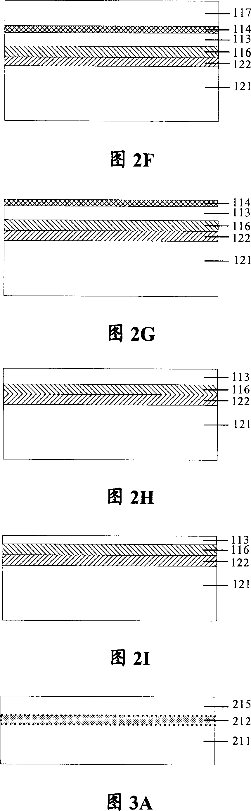
[0136] In this embodiment, the surface silicon layer is the sum of the first surface silicon layer 215 and the second surface silicon layer 217 shown in FIGS. 3A to 3J , and the insulating layer is the third insulating layer 218 .

[0137] Referring to FIG. 3A, it is a schematic diagram of the cross-sectional structure of the silicon wafer after implanting ions capable of reacting with silicon to form a corrosion barrier material on the silicon wafer. As shown in the figure, after the ion implantation, an ion implantation layer 212 is formed in the silicon wafer. The ion implantation layer 212 divides the silicon wafer into a first surface silicon layer 215 and a substrate silicon layer 211 . The ions implanted on the silicon wafer that can react with silicon to form corrosion barrier materials are nitrogen ions or oxygen ions, or other ions such as carbon ions. Generally speaking, the basic principle for selecting implanted ions is the ions formed after ion implantation The i...


PUM

PropertyMeasurementUnit
thicknessaaaaaaaaaa
thicknessaaaaaaaaaa
thicknessaaaaaaaaaa

Abstract

The invention is concerned with the silica isolator manufacturing method, it is: injects the silica sheet with the ion that effects with the silica to form the corrosion preventing material; annealing the silica and forms the structure with the isolating layer, on the outside of the sheet , places next to the silica surface layer, the corrosion preventing layer places next to the silica substrate layer, which is, too, on the outside of the silica sheet; next, forms the second isolating layer on the semiconductor wafer; attaches silica sheet with the wafer to join the isolating layer with the second isolating layer; reinforces the attachment; wipes off the silica substrate layer; and wipes off the corrosion preventing layer too. The invention produces the silica isolator with adjustable thickness, the better quality isolating layer, and the top layer silica is equally thick.

Description

technical field [0001] The invention relates to a silicon-based integrated optoelectronic device material and its preparation process, in particular to a silicon-on-insulator and its preparation process, belonging to the technical field of microelectronics and solid electronics. Background technique [0002] Silicon-on-insulator (Silicon-on-insulator, SOI) is a new type of semiconductor material, which mainly includes top silicon, buried oxide layer (Buried oxide layer, BOX) and supporting substrate in structure, where the buried insulating layer is located between the top layer of silicon and the supporting substrate. The conventional buried insulating layer material is silicon dioxide. The above-mentioned structure of silicon on insulator can completely isolate the device on the top layer of silicon from the supporting substrate material, substantially reduce junction capacitance and leakage current, increase switching speed, reduce power consumption, and realize high-spe...

Claims


Application Information

Patent Timeline
Patent Type & Authority Applications(China)
IPC IPC(8): H01L21/84H01L21/762H01L21/20H01L21/00H01L27/12
Inventor 陈猛
Owner SHANGHAI SIMGUI TECH
Why Eureka
Try Eureka