Novel process for producing microcolor filter array

A filter array, filter technology, applied in the direction of filter, photolithography process of pattern surface, metal material coating process, etc., can solve incompatibility, limit the further improvement of integration, micro-filtering The edge of the film is uneven and other problems, so as to achieve the effect of improving the accuracy and the edge effect.

Inactive Publication Date: 2008-01-16
JINGYING OPTICS
View PDF2 Cites 11 Cited by
  • Summary
  • Abstract
  • Description
  • Claims
  • Application Information

AI Technical Summary

Problems solved by technology

[0003] The above-mentioned process has achieved great success, but with the further improvement of technical requirements, especially the further improvement of the integration and quality requirements of the above-mentioned micro-filter array, the above-mentioned process has exposed its serious defects
Mainly include: 1) The traditional optical coating technology (electron beam evaporation) does not match the modern semiconductor technology, especially the VLSI semiconductor technology. The technical requirements of the two are very different in cleanliness and other aspects. Compatible, unable to build a complete production line; 2) The traditional lift-off process, because the photoresist has a certain height, will form a shadow on its edge, when using the traditional electron beam evaporation process, it will affect the thickness of the deposited film edge shadow effect
In addition, the lift-off process itself can cause irregularities at the edges of the microfilters
All these limit the further improvement of its integration

Method used


Image

  • Novel process for producing microcolor filter array
  • Novel process for producing microcolor filter array
  • Novel process for producing microcolor filter array

Examples


Embodiment Construction

[0012] Specific embodiments of the present invention will be described below with reference to the accompanying drawings.

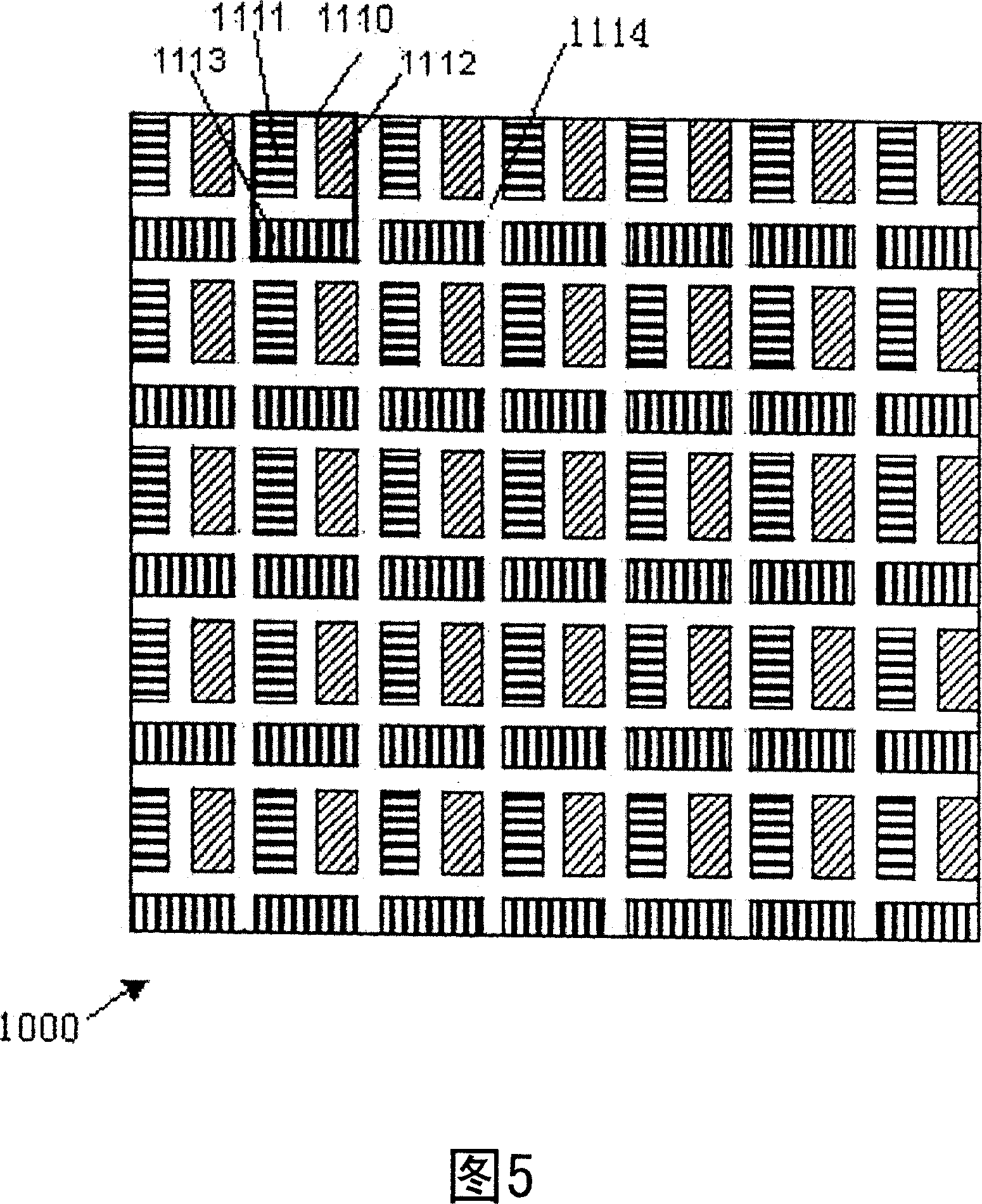
[0013] Figure 5 illustrates an example of a microfilter array that can be used for color LCoS. The micro filter array 1000 is composed of many basic units 1100 evenly arranged, and each basic unit 1100 is composed of three different optical filters, namely blue filter 1111, green filter 1112 and red filter. sheet 1113, and a certain gap 1114 is left between each filter. The processes of the following embodiments will be illustrated by making the example shown in FIG. 5 . Of course, these processes can also be used to fabricate other types of microfilter arrays.

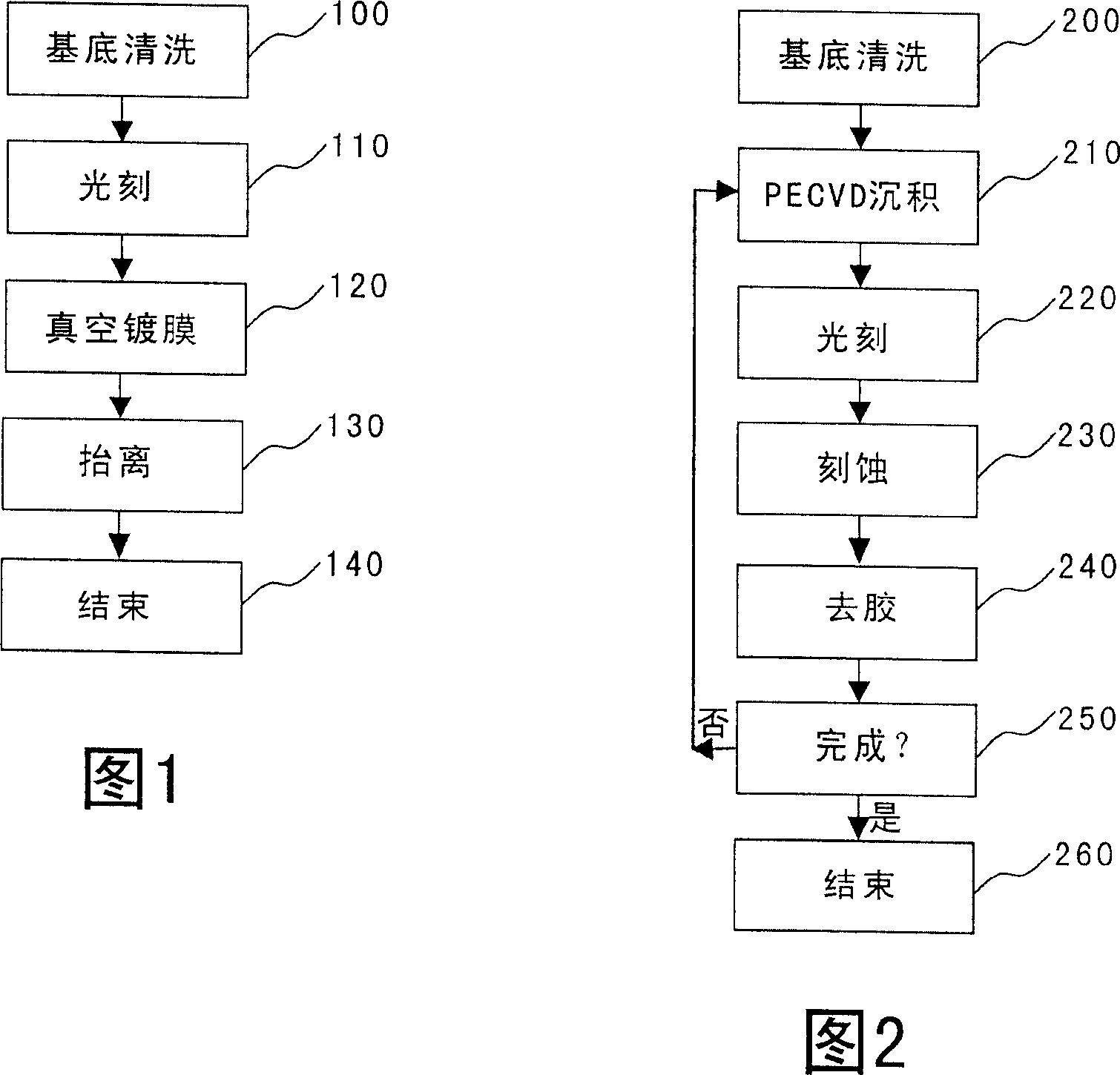
[0014] Figure 2 illustrates a novel process for fabricating a microfilter array according to the present invention. As shown in FIG. 2 , in step 200 , substrate cleaning is performed, and the substrate cleaning in step 200 is basically the same as that in step 100 . In one embodiment, the sub...


PUM

PropertyMeasurementUnit
thicknessaaaaaaaaaa
thicknessaaaaaaaaaa
thicknessaaaaaaaaaa

Abstract

The invention discloses a new technique used to manufacture microfiltration optical lens array which comprises the following steps: a base is cleaned up; multi-layer films of Si3N4 and SiO2 are deposited alternatively by the sediment method that chemical gas phase is enhanced by plasma; photoetching; a photo resist is taken as a mask; multi-layer films of Si3N4 and SiO2 are etched and striped; wherein the steps including sediment, photoetching and etchant can be repeated, and hence microfiltration optical lenses and arrays in different catalogs and patterns which are needed are obtained.

Description

technical field [0001] The present invention generally relates to a new process for fabricating micro-filter arrays, and in particular, relates to a new process for fabricating micro-filter arrays using PECVD. Background technique [0002] Optical thin films are an extremely important part of modern optical engineering. It can be said that any optical system is inseparable from the existence of optical films. Moreover, with the development of modern optical technology, new challenges are also presented to optical thin film technology. For example, with the miniaturization, miniaturization, and integration of modern optical systems, the requirements for miniaturization, integration, and patterning of optical films are also put forward. For example: the projection system mentioned in U.S. Patent 6,987,579 uses an SCR color filter color wheel, which requires the edge profile of each filter to conform to the Archimedes spiral; another example: Chinese patent ZL02 217356.0 pro...

Claims


Application Information

Patent Timeline
Patent Type & Authority Applications(China)
IPC IPC(8): G02B5/20G03F7/00C23C16/44
Inventor 樊斌邵剑心
Owner JINGYING OPTICS
Why Eureka
Try Eureka