

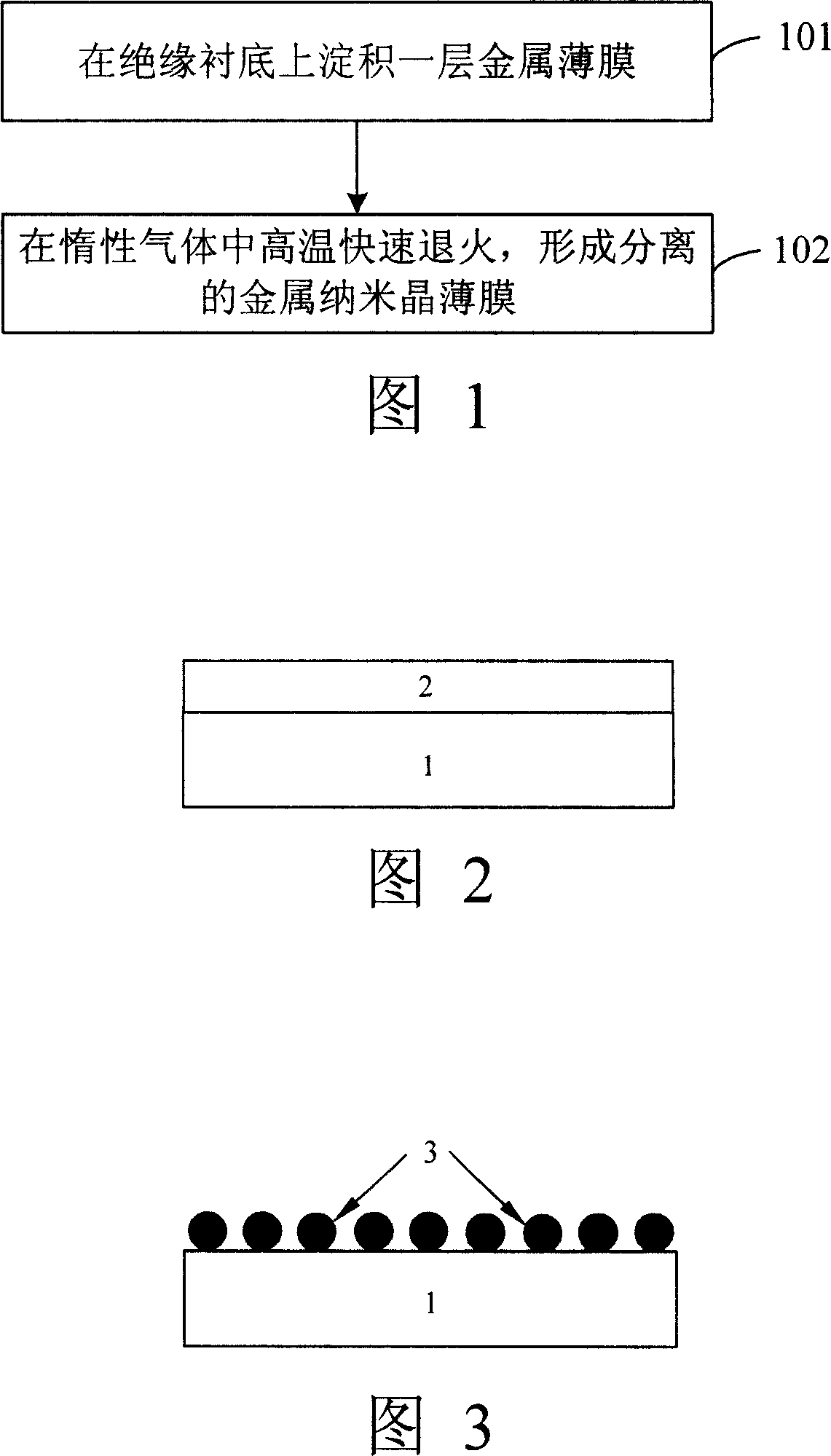
Method for preparing metal nano-crystal thin film
A metal nanocrystal and metal thin film technology, which is applied in metal material coating process, vacuum evaporation plating, coating, etc., can solve the problems of complex preparation process of metal nanocrystal material, poor compatibility of silicon plane process, single material type, etc. , to achieve the effects of improving process stability and preparation efficiency, good charge trapping and storage characteristics, and simplifying the preparation process
- Summary
- Abstract
- Description
- Claims
- Application Information
AI Technical Summary
Problems solved by technology
Method used
Image

Examples
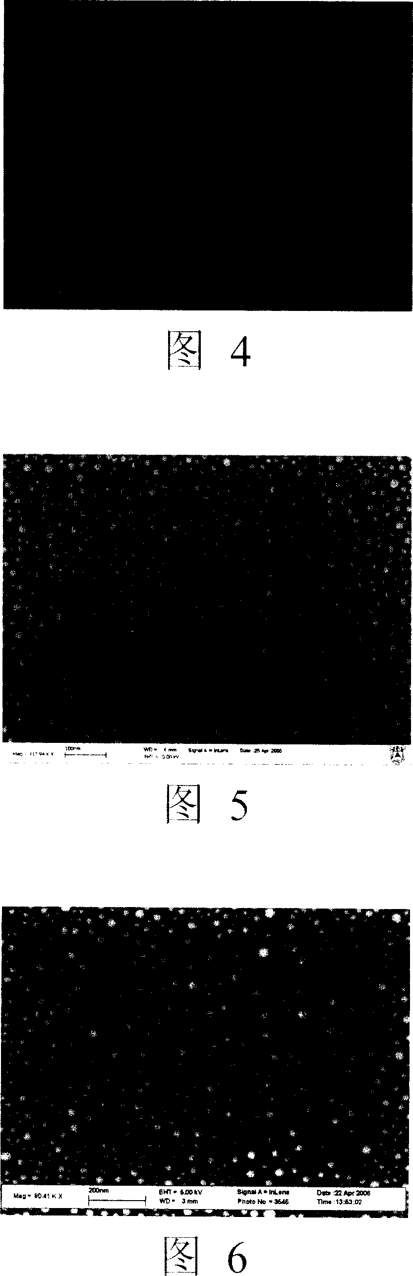
Embodiment 1
[0043] Growth of a layer of SiO on Si substrate by thermal oxidation 2 insulating dielectric, and then use magnetron sputtering on SiO 2 A layer of 2 to 3nm thick Ni metal film is grown on the insulating medium, and finally on the N 2 Rapid annealing at 800°C for 30 seconds to form a Ni nanocrystalline film. As shown in FIG. 4 , FIG. 4 is a scanning electron micrograph of a Ni nanocrystalline film prepared according to the first embodiment of the present invention. In Fig. 4, the diameter of Ni nanocrystals is 5 to 20 nm, and the density is 3×10 11 / cm 2 .
Embodiment 2
[0045] Growth of a layer of SiO on Si substrate by thermal oxidation 2 insulating dielectric, and then use magnetron sputtering on SiO 2 A layer of WSi with a thickness of 2 to 3 nm is grown on the insulating medium 2 metal film, finally in N 2 rapid annealing at 1100°C for 30 seconds to form WSi 2 nanocrystalline film. As shown in Figure 5, Figure 5 is a WSi prepared according to the second embodiment of the present invention 2 Scanning electron micrographs of nanocrystalline thin films. Figure 5, WSi 2 The diameter of nanocrystals is 10 to 30nm, and the density is 1×10 11 / cm 2 .
Embodiment 3
[0047] Growth of a layer of SiO on Si substrate by thermal oxidation 2 insulating dielectric, and then use magnetron sputtering on SiO 2 A layer of WTi metal film with a thickness of 2 to 3 nm is grown on the insulating dielectric, and finally the 2 Rapid annealing at 800°C for 30 seconds to form a WTi nanocrystalline film. As shown in FIG. 6 , FIG. 6 is a scanning electron micrograph of a WTi nanocrystalline thin film prepared according to the third embodiment of the present invention. In Fig. 6, the diameter of WTi nanocrystal grains ranges from 10 to 40 nm, and the density is 1.5×10 11 / cm 2 .
PUM
| Property | Measurement | Unit |
|---|---|---|
| Diameter | aaaaa | aaaaa |
Abstract
Description
Claims
Application Information